Many electronic systems require voltage gain, current gain or in general power gain. Note that voltage gain or current gain larger than unity can easily and linearly be achieved using passive components such as capacitors and inductors or with transformers. However, if power gain larger than one is required then components that can be used to achieve that power gain larger than 1 must be used. It was already explained in Chapter 1 that this requires non-linear two port devices; in this book we assume BJTs and MOS transistors for this.
In this chapter and in chapter 5, we aim at linear amplifiers31 . Linear amplifiers are basic building blocks for many electronic systems. Non-linear amplifiers are also widely applied in e.g. digital circuitry, mixers that serve to shift signals in the frequency domain and in circuits that do analog-to-digital conversions, but these are usually extensions of linear(ized) amplifiers, and are not addressed in this book.
Using the nonlinear element equations of MOS transistors or BJTs in analyses typically creates cumbersome calculations, and at best yields huge equations that offer very limited insight. Only for relatively simple circuits, closed form expressions that relate e.g. output voltage to input voltage can be derived. One example of this is given below.
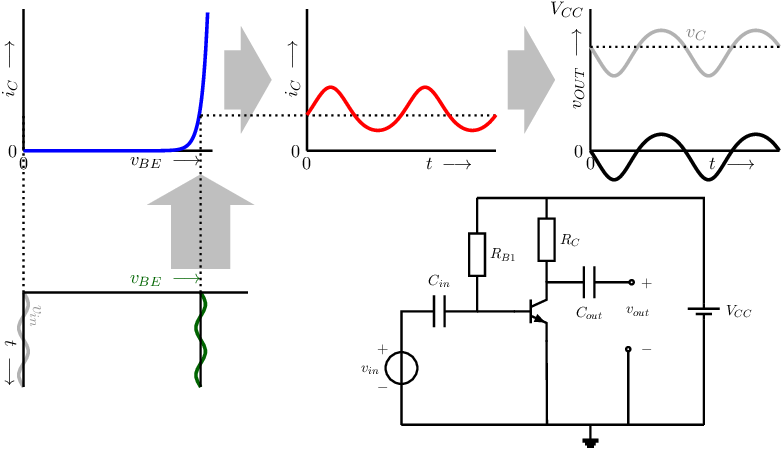
In Figure 4.1, the circuit schematic is shown in the lower right hand side corner. The input signal and the voltage-shifted are shown as a function of time in the lower left hand side graph. Note that this plot is rotated to be able to (below) construct and graphically. The resulting can be constructed graphically by mirroring the signal in the curve. The voltage at the collector and the (DC-free) then follow by applying Ohm’s law; these are shown in the rightmost graph.
For this quite simple circuit, the voltage at the collector node, due to the sinusoidal can be derived mathematically. Note that the output voltage has the same shape as if this circuit is unloaded, but that it may be DC-shifted due to the presence of .
For more complex circuits, deriving the exact relation between an input signal and an output signal gets quite complicated, resulting in useless relations (in the sense that they do not give any comprehensible insight). From a fundamental point of view, properties such as input impedance, output impedance and circuit bandwidth cannot be derived or defined as these hold for linear(ized) circuits.
Aiming at linear circuits, typically all kinds of linear properties of a circuit are of interest. These include the aforementioned transfer functions, input and output impedances, bandwidths, and more. Being properties of linear circuits, at least many of these are defined in the frequency domain and in impedances. This requires to analyze the linear part of the behavior of a circuit of interest and to regard any deviation from linear behavior as non-ideal.32 . Getting the linear-only part of (4.1) can be done in multiple ways:
Note that both approaches of using linearising gives us:
a reasonable (linear) approximation of the behavior of the nonlinear component or circuit around some bias point,
a limited validity of the results. It follows directly from series expansions that the accuracy of the linear approximation decreases with increasing signal excursions about the bias point and decreases with less-linear element equations.
whereas the upfront linearization approach gives us:
a linear circuit that can be easily analyzed,
equations that can be interpreted (hence relations),
insight.
From this is may be clear that the preferred way to analyze linear(ized) behavior of circuits is to apply upfront linearization. after which any linear analysis method in time domain or in frequency domain can be used.
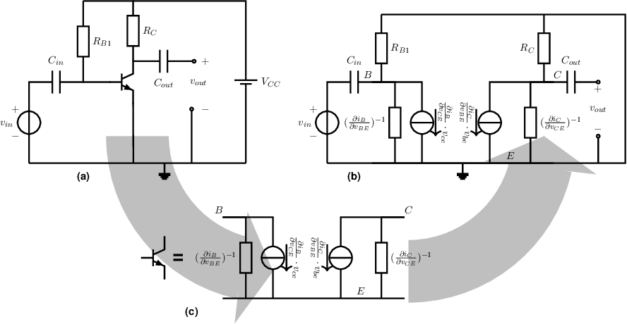
The circuit we obtain after replacing all nonlinear components by their linear approximation using a Taylor series expansion is called the “linear equivalent circuit”. Note that the linear equivalent circuit that contains many DC sources ( order Taylor terms) and many linear impedances and many linear controlled sources ( order Taylor terms). For the circuit in Figure 4.2(a) and the replacement of the BJT by its linear equivalent in Figure 4.2(c) yields the linear equivalent circuit in Figure 4.2(b).
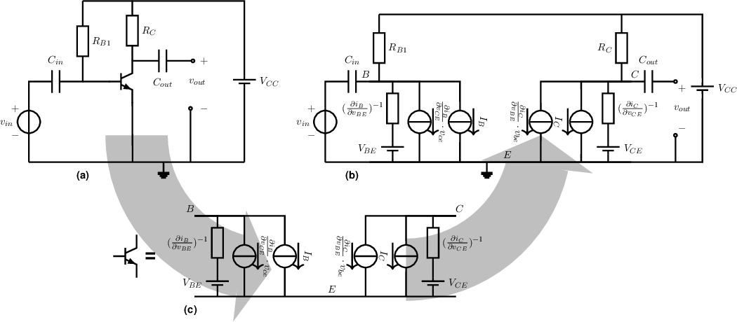
In the linear equivalent of the BJT, the full first order series expansion of the BJT is used. This includes DC-voltages, DC-currents and the four partial derivatives of the two port currents to the two port voltages. The DC sources in this equivalent circuit are only relevant for the DC levels of currents and voltages of the circuit and are hence irrelevant for signal properties33 .
In the circuit on the left hand side of Figure 4.2, the BJT is replaced by a order Taylor expansion to get the linear equivalent circuit on the right hand side. In that linear equivalent, the DC contributions are irrelevant for derivation of signal transfer, input impedances, output impedances, ... and can be freely omitted34 . To analyze (or synthesize) the behavior of circuits for signals, it can be concluded that only the first order Taylor series expansion terms are of interest. Higher order terms and zero-th order terms are then irrelevant.
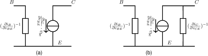
The equivalent of a non-linear component or non-linear circuit that only includes the first order series expansion terms is called a small signal equivalent circuit. For the circuit in Figure 4.3(a), the BJT should then be replaced as shown in Figure 4.3(b).
In the small signal equivalent shown in Figure 4.3(c), also the first order-only expansion terms for the other components are used.
For the resistors and capacitors, the first-order only equivalent equals their resistance respectively capacitance.. Independent signal sources that actually provide a signal are kept in.
Independent DC-sources do not provide any signal: they provide a DC level of voltage or current. In the circuit in Figure 4.3(c) these DC sources are replaced by their impedance at signal frequencies. DC-voltage sources then translate into a short () while DC-current sources translate into an open (). The small signal equivalent circuit hence does not include any DC-source.
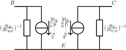
A small-signal equivalent circuit of a BJT follows from the most general expression for the base current and collector current of a BJT. Shown below is the derivation for NPNs.
The element equations for an NPN are shown in (4.2) and (4.3). The rightmost term in (4.2) models an unwanted dependency of on , using the so-called Early-voltage .
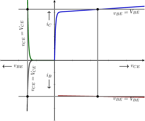
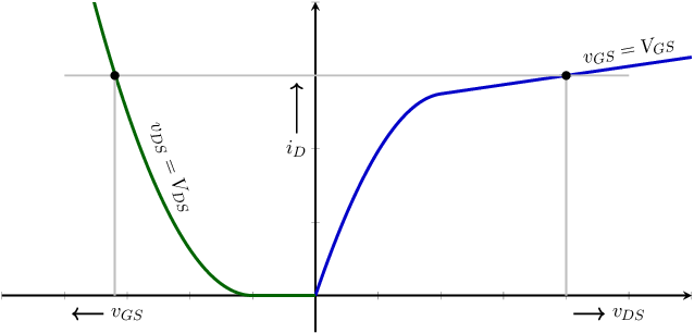
Note that the NPN is usually operated with where the second term between brackets is close to one and hence can be neglected. Figure 4.4 shows actually 4 graphs to capture the most relevant i-v relations of an NPN in a specific operating point in one figure. For readability the numbers on the axes (and the units) are omitted and the axis and axes are scaled differently for the same reason.
is shown in the first quadrant, for the
in the operating point.
Note that the x-axis represents
whereas the y-axis corresponds to .
for the
in the operating point is shown in the second quadrant.
For this quadrant, the x-axis to the left corresponds to .
for the
in the operating point is depicted in the
quadrant.
The downward y-axis corresponds to
and is differently scaled as the -axis
for readability.
for the in the operating point is in the forth quadrant. For this curve, a small dependency of on is assumed.
The bias point for this transistor is marked by the (4) dots that correspond to the voltages and current combinations in that bias point: , , , and respectively. The lightgray vertical and horizontal lines ’“connect” these 4 points for illustration reasons.
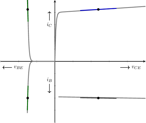
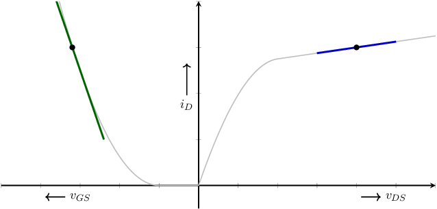
A Taylor expansion for and about the bias point respectively then gives:
The zeroth-order terms correspond to the bias point settings, and hence correspond to the dots in Figure 4.4 and in Figure 4.5. The zero-th order terms and the first order terms combined represent “first-order” or linear approximations about the bias point. Figure 4.5 shows the transistor’s i-v-characteristics in gray, the bias point as dots and shows the linear approximation of the i-v-curves about the bias point as thick line segments.
The difference between the actual transistor behavior — the actual non-linear i-v-characteristics — and the linear approximation is small for small (in voltage and current) excursions about the bias point. Mathematically they are described by the sum of all higher order terms in the Taylor series expansion. In so-called small-signal analyses and in small-signal operation of a circuit, it is assumed that the linear approximation is sufficiently accurate.35
For small variations, the terms ( and () can be replaced by their differential notations; and . This can be written even shorter by replacing the differential terms by “small-signal symbols”: for example the base voltage variation and the collector current variation . Taking into account only the terms that describe the variations — the first order terms in the expansion — this yields
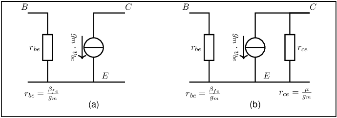
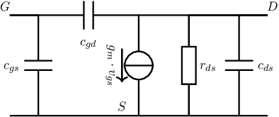
The small-signal equivalent circuit (SSEC) of an NPN, corresponding to the equations in (4.4), is shown in Figure 4.6.
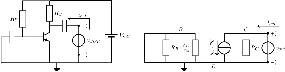
With the SSEC of an NPN as in Figure 4.6, to construct a SSEC of a circuit, every NPN should be replaced by 2 resistors and 2 voltage controlled current sources. This means that the SSEC contains many more components than the original circuit. The advantage is of course that the SSEC is linear whereas the original circuit was inherently nonlinear. For most applications, using the full SSEC of an NPN is not necessary: some components may be neglected and hence may be left of the SSEC. The next list enumerates the components in descending order of importance:
the controlled output current is THE reason to use a transistor: it may not be left out except if you’re modelling a destroyed transistor. The current variation forced by this source equals .
the base current is just as fundamental, but unwanted. The (small-signal) base current as a response to a (small-signal) base-emitter voltage corresponds to the resistor between B and E and can not be omitted.
the output resistance, the resistor between C and E, only is relevant if an external load impedance of the BJT is high ohmic compared to the transistor’s output impedance. Only in that case the transistor’s output resistor must be included, and it can freely — and should to limit calculation complexity — be excluded otherwise.
the input current as a result from output voltage variations is usually small and can usually be neglected.
Hence the SSEC to be used is usually the one shown in Figure 4.7a. Only if the load of the transistor is very high ohmic (such as using a DC current source as load) then the SSEC in Figure 4.7b should be used.
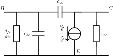
The notation used in (4.4) and in Figure 4.7 is not that easy to read. For that reason meaningful short hand notations are introduced for some properties of the components in the SSEC of the BJT:
the main use of the BJT is to create an output current variation from its input voltage variation. The ratio between the two is called the transconductance :
|
| (4.5) |
the base current is fundamental, and is a factor “current gain” or smaller than the output current. Consequently the corresponding resistor between B and E has a value:
|
| (4.6) |
in many applications, achieving a high voltage gain is very important. It can be derived that the maximum achievable voltage gain factor using passive load impedances equals the product of the and the transistor’s output resistance ; for this product the symbol is frequently used, leading to:
|
| (4.7) |
Using these short hand notations, the resulting SSEC for a BJT is shown below. As stated before, the most simple version that can be used, should be used. This usually means that the SSEC of choice consists of only 2 linear components: the voltage controlled current source that represents the essence of the transistor and the input resistor that represents the fundamentally present main unwanted effect: input current.
Note that the above derivations of small signal equivalents was done for NPN transistors. For the PNPs the derivation is very similar. To recap, the element equation of PNP are the same as those for an NPN — listed in (4.8) and (4.9) — except for the sign of the terminal currents and the sign of the port voltages:
Note that whereas for NPNs, for PNPs . Likewise, the early voltage is positive for an NPN and negative for a PNP.
Having the exact same element equations but with current signs and voltage signs opposite from those for NPNs, the derivatives are the same for NPNs and PNPs. The small signal equivalent of a PNP is hence identical to that of an NPN, and hence is also depicted in Figure 4.8.
The previous section described the (linear) small-signal equivalent circuit for a BJT; the work in that section is repeated here to get the SSEC for a MOS transistor. Starting with the element equations of an NMOS transistor (the drain current equations are for strong inversion saturation and strong inversion linear region respectively):
In the expression for the saturation region, the term models the unwanted dependency of on via ; this term is only relevant if the external load impedance of the MOS transistor is high ohmic compared to the transistor’s output impedance. In all other cases we can freely neglect this term.36 . Similar to what was done in $4.4, Figure 4.9 shows 2 graphs to capture the most relevant (DC) i-v relations of a MOS transistor in a specific operating point in one figure.:
for the in the operating point; this curve is shown in the first quadrant.
for the in the operating point; this curve is shown in the second quadrant.
The bias point for this transistor is marked by the (2) dots that correspond to the voltages and current combinations in that bias point: and respectively. The light-gray horizontal lines ’“connect” these two points for illustration reasons.
The SSEC for the MOS transistor now follows from a first-order Taylor series expansion:
The zeroth-order series expansion terms are the bias point settings, and correspond to the dots in Figure 4.9. The zero-th order and the first order terms together form a linear approximations about the bias point. Figure 4.10 shows the transistor’s i-v-characteristics in gray, the bias point as dots and shows the linear approximation of the i-v-curves about the bias point as thick line segments.
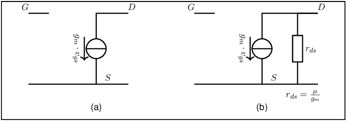
Just like BJTs and vacuum tubes, a MOS transistor behaves essentially a voltage controlled current source. The parameter is the most important small-signal parameter; just like for the BJT this parameter is called transconductance . The parameter corresponds to the output conductance and is denoted with the symbol ; this output conductance can also be written as an output resistance . For small-signals (variations) in drain current:
|
| (4.12) |
where in saturation
These SSEC parameters are specific for the bias point for the transistor: the SSEC parameters follow from a Taylor series approximation about the bias point. Because of this, in the equations above, and . The resulting small-signal equivalent circuit of an NMOS transistor is shown on the left hand side in figure below. The effect of the output resistance is often neglected; in this case the SSEC for an NMOS transistor can be simplified to that on the right hand side in the figure. Similar to the situation for NPNs and PNPs, the small signal equivalent circuit of a PMOS transistor is equal to that of an NMOS transistor.
For calculations using the SSEC of a BJT or MOS transistor, the various small-signal parameters (mainly the , the and only the or when required) must be known. These small-signal parameters follow from the bias point and the element equations.
The most important small-signal parameter of the BJT is the change in collector current due to a change in the base-emitter voltage : represented by the transconductance . From its definition and the element equation for an NPN transistor we get:
where the first small signal element equation includes a (small) dependency on . For the PNP the same equations result. Whenever possible the second — simplified — small signal element equation will be used. It can be seen that the transconductance of a BJT is proportional to its DC (bias) current . For the :
The output resistance of a BJT — — follows from the element equations and the bias conditions as well. However in this book we use either a prespecified or a value related to a prespecified maximum achievable gain: .
For the MOS transistor, similar quite simple relations can be derived for the small-signal parameters. From the element equations for an NMOS transistor, for operation in strong inversion and saturation (for now the linear region is neglected):
The most essential parameter — the transconductance — can be calculated to be . The last term in this expression is preferably neglected, yielding . This follows from the in the bias point (and in the bias point if we have to include a finite output resistance) and from the transistor property . Reusing the transistor’s element equation, this equation for can be rewritten into 3 useful forms that can be used to calculate the transconductance:
Which of these equations is most useful depends entirely on which properties are known; usually 2 out of the 3 possible parameters are known and can be substituted in one of the 3 -equations. The equations for PMOS transistors are identical.
Charge storage in transistors: small signal capacitances
As explained in chapter 2, there is charge storage in every junction that is non-linearly dependent on the voltage drop across the junction. Small signal wise, this translates into having to associate a small signal capacitance with every junction.
For BJTs this corresponds to 2 small signal capacitances, one associated with the B-E-junction and one associated with the B-C-junction. As explained in chapter 2 these capacitances are bias point dependent. A more accurate small signal equivalent model for BJTs, then the ones introduced earlier in this chapter — still neglecting the term — is then
For MOS transistors, in this book it is assumed that the source and bulk are tied together, see e.g. $2.5. As a result, only one junction — the drain-bulk-junction — is present in the MOS transistors in this book. Apart from that, MOS transistors fundamentally operate by creating/modulating an inversion layer between source and drain, using the gate (voltage). This translates into charge storage associated with both the gate-source voltage and associated with the gate-drain voltage. Small signal wise, this may be modelled as a gate-source capacitance and a gate-drain capacitance., both being bias-dependent. A more accurate small signal equivalent model for MOS transistors than the ones introduced earlier is then
No in-depth analyses nor descriptions concerning these capacitances will be given in this book - that is considered outside the scope of this book.
Elaborate small signal models for transistors
Elaborate small signal modes — are used for e.g. very accurate calculations and for simulations — include many more small signal components. These models follow from equations describing the node currents as function of all node voltages and from the equations that describe charge storage in transistors by charge assigned to each node, as a function of all node voltages.
For a BJT these equations are then, very much simplified:
which leads to
(trans)conductances and to
(trans)capacitances .
Note that e.g. a transcapacitance in general is not equal to : the change in (here) gate charge due to a drain voltage change can be completely different from the change in drain charge due to a gate voltage change. The same holds of course for transconductances and for all : they are not identical. In the small signal models that are suitable for hand derivations, quite significant simplification are introduced leading to the models presented earlier in this chapter.
One of the 3 node voltages can be seen (or denoted) as a reference voltage, which results in quite some redundancy in the
(trans)conductances and
(trans)capacitances. It can
readily be seen that deriving the
and for 2
nodes, regarding the other node as reference is sufficient to describe all small signal properties. Hence the full set of
transcapacitances and
transconductances can also
be uniquely described by
transcapacitances and
transconductances.
For a MOS transistor, in this book a 3-terminal device is assumed for simplicity reasons: the bulk and source terminals are assumed to be shorted. In a more general notion this is not the case and the node current and node charge can be defined for all 4 nodes. In a way that is similar to that for BJTs this leads to
(trans)conductances and to
(trans)capacitances .
where . Again, there is quite some redundancy in these transcapacitances and transconductances. Using one of the nodes as reference (usually the bulk or source is used for that), unique transcapacitances and unique transconductances follow that are sufficient to describe all small signal parameters.
It was demonstrated in chapter 3 that a transistor needs proper biasing — in some DC bias point — to be able to perform. The current chapter deals with small input signal variations about the bias point to get some output current variations that can — using Ohm’s Law — be transformed into output voltage variations. It is hence crucial that transistors in a specific circuit are both properly biased at a DC level, that AC input signals can be applied to the transistors and that the resulting AC output signal can be used in some way.
In a real circuit applying variations onto the input of a transistor can be done in multiple ways:
the most easy way may seem driving a transistor with a series connected DC voltage source and AC signal source. However, putting two voltage sources in series proves to be hard in actual circuitry.
something else
One of the most straightforward ways of that “something else” is used throughout this book. Noting that the bias voltage is fundamentally DC and a signal is fundamentally AC opens possibilities to add voltages. This is worked out using a circuit in Figure 3.5b, now used to amplify an input voltage :
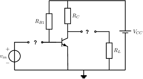
Coupling the AC voltage source directly between B and E would prevent (independent of the input signal) realising a suitable bias point for the transistor: replacing the “?” by a short will not work out nicely. Elaborating a little leads to a number of requirements for coupling the input signal to the input terminals of the transistor:
coupling the input signal may not disrupt the DC bias of the transistor
the input signal must, preferably, not be attenuated by the coupling
This seems to be a contradiction: on one hand, the input signal should be coupled onto the transistors’ input terminals, while on the other hand it shouldn’t. The solution is to satisfy both requirements at the same time, but not for the same frequency. We can now redefine the requirements:
for DC, the coupling component must have a high impedance in order not to disturb or compromise proper (DC) biasing settings
for signal frequencies, the coupling component must have a low impedance
Again, there are multiple solutions to this problem. Firstly, an inductive bias circuit can be used in combination with a signal source that has a non-zero series resistance. This type of solution is mainly used in circuits operating at very high frequencies. Firstly, a coupling component that is high ohmic for and that is low ohmic for signal frequencies can be used. This can be accomplished by a capacitor as coupling component. The capacitive coupling is used almost exclusively in this book.
With capacitive coupling, the value of the capacitor is not relevant for blocking of the DC current: the impedance of any capacitor is infinite for DC signals. For passing the AC voltage from the source to the amplifier, the value of the capacitor is most definitely of importance as it forms — together with the input resistance of the circuit — a first-order high-pass characteristic. If the -3dB corner frequency of that characteristic is sufficiently below the lowest signal frequency the coupling can be considered good for any signal frequency37 .
Example For an amplifier with an input resistance of =1 k and an input signal frequency range from 20 Hz to 20 MHz:
if the attenuation due to the coupling has to be smaller than 3 dB, a minimum value for the coupling capacitor follows the signal transfer function:
Being in a standard form for a first order high pass function (see section 0.14), it directly follows that and hence
if the amplifier has to settle within 1% of its bias within 1s after switching on source, the maximum value for the coupling capacitor is:
To calculate small-signal properties of circuits — such as input impedance, output impedance, bandwidth or signal gain —first we need an SSEC of the total circuit. Whereas the circuit itself comprises transistors, sources, passive components and more, its small signal equivalent circuit is the first order only representation of the original circuit. This (linear) SSEC then can be analyzed using all the theorems, rules, tips and tricks of linear network analysis.
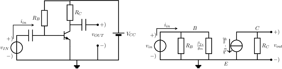
As example, after creating an SSEC for the circuit in Figure 4.12, a few derivations of small-signal parameters are shown. Figure 4.13 shows a step-by-step derivation of an SSEC.
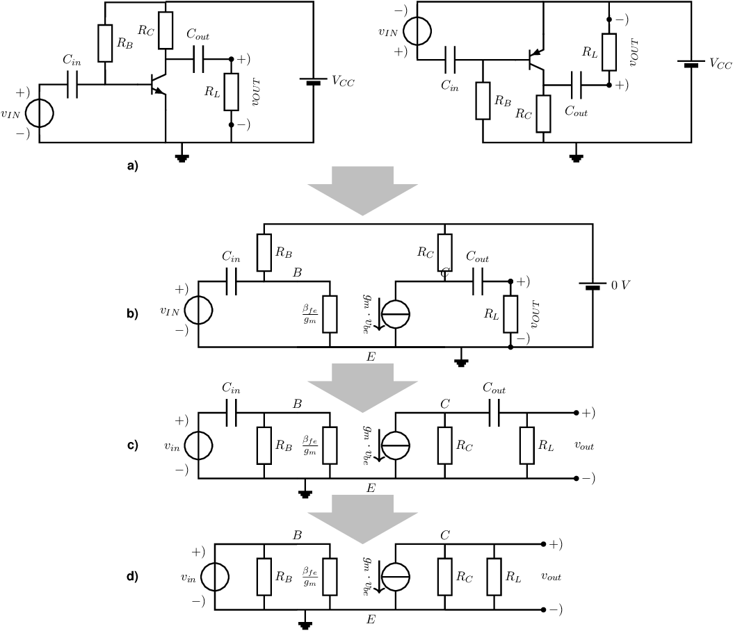
In the first step components are replaced by their small signal equivalents. For this particular circuit, the BJT is replaced by its SSEC and DC sources are set to 0. When replacing non-linear components by their SSEC it is very important to keep track of the original position of (here) the base, collector and emitter terminals.
The second step is redrawing and simplifying the SSEC obtained after the first step: this usually boils down to plain redrawing and redrawing... To reduce complexity in this step, parallel impedances may be merged into single equivalent impedance. The SSEC in Figure 4.13c is a small-signal equivalent of the circuit in Figure 4.13a that can be used to calculate any small signal property of the original circuit. In this example these properties are frequency-dependent gain, input impedance and output impedance.
Usually it is implicitly assumed that coupling capacitances are sufficiently low ohmic at signal frequencies. In this context “sufficiently low ohmic” means that at signal frequencies the voltage drop across the capacitors is negligibly small and hence the capacitors can then be modelled as shorts. In that case the SSEC in Figure 4.13c can be simplified to the SSEC in Figure 4.13d.
Using the SSEC in Figure 4.13d, now a few small-signal properties will be derived for the circuit in Figure 4.13a:
input impedance
The input impedance of an amplifier is the impedance we “see” looking from the controlling
source “into” the input port of the circuit. According to Ohm’s law ,
or for a purely resistive input impedance .
Deriving
can be done in many ways, relatively easy ones being driving the input of the circuit with a small
signal voltage source
and calculating the resulting
or driving
and calculating .
The ratio of the two yields .
For the SSEC in Figure 4.13d and hence for the circuit in Figure 4.14 this yields .
output impedance
The output impedance of the amplifier is the impedance “seen” when looking “into” the
output port of the circuit. Similar to the derivation of input impedance, output impedance is
when driving the output port by either a voltage source
or by a current
source .
Note that any other signal source should be set to 0 in this case. Another method that
does not require introducing an output port driving source, but that requires an input signal
source, is loading the output of the amplifier by two different impedances deriving
from he resulting output voltages and/or output currents. In the limit case an infinite load
impedance (an open) and a zero load impedance (a short) may be used, leading to
.
In this book usually the output port is driven by a signal source, having all other independent signal set to zero, and calculating . An example of this is given in Figure 4.15, yielding .
voltage gain:
The voltage gain (i.e. voltage amplification factor) of the amplifier can readily be evaluated — from Figure 4.14 —
to be .
To derive small signal properties of circuits including other types of non-linear components, such as MOS transistors, the same approach can be applied. The MOS equivalent of the amplifier in Figure 4.14 and its SSEC are shown in Figure 4.16.

Using the SSEC, we can readily derive that the input impedance is , that the voltage gain equals and that (using a little modified SSEC — driving the output port and setting all other independent sources to 0) the output impedance is equal to .
We want to design an amplifier with a BJT that has a voltage gain of . Note that the basic amplifier circuit of Figure 4.13a is an inverting amplifier for which . Usually it is not relevant whether an amplifier is inverting or not, as long as we’re only interested in voltage gain. Then we can use which directly leads to requiring =100. Using
where is the collector bias current level, it follows that the voltage drop across equals which amounts to 2.58V at room temperature. Ignoring non-linear effects — hence assuming sufficiently proper small signal behavior — the supply voltage needs to be high enough to support
,
a minimum to keep the BJT in active forward operation
a voltage amplitude at the collector node .
Note that when assuming a linearized equivalent of the amplifier, the input signal magnitude to keep the linearized collector current positive and to keep the collector voltage positive. The minimum supply voltage for our CEC amplifier then equals
For the collector current changes quite a lot: by up to a factor larger or smaller than the bias current which implies that the operation of the BJT is not small signal and therefore may not be sufficient linear. To get sufficiently linear behavior of this amplifier, the input signal must be sufficiently small to ensure that the variation in collector current () is much smaller than the DC bias collector current . For this circuit, this can be translated in accepting only input signal voltage levels up to a few mV (depending on linearity or distortion demands).
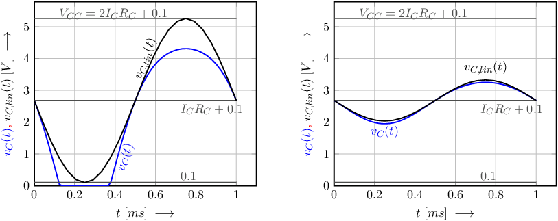
The graphs below show the BJT’s collector voltage and the linearized for a CEC designed for , , maximum using the corresponding minimum , and . In the graph on the left , while in the graph on the right .
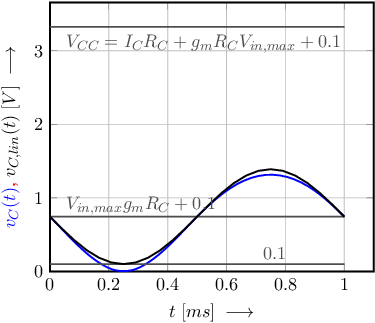
If the input signal amplitude is known to be smaller than , the minimum required supply voltage can be lowered with respect to the situation in the previous two graphs. Assuming a maximum and adjusting the supply voltage to the corresponding minimum :
Using more complex circuit topologies, the gain-supply voltage trade off can be circumvented: then high gain at low supply voltage can be obtained. For this, typically multiple amplifier stages are cascaded. Also the requirement that the input voltage be restricted to several mV to get sufficiently linear behavior can be circumvented. This is usually at the cost of extra components, and requires feedback which in turn usually comes at the cost of power consumption and a lower maximum frequency of operation. These are topics of upcoming chapters in this book.