Chapters 6-10 analyzed, synthesized and showed a lot of circuits that use operational amplifiers (opamps). In those chapters, a lot of attention was paid to the external behaviour (bandwidth, amplification, output impedance, etc) of an opamp, but little to none went into their internal structure. In this chapter, the internal circuits of opamps are discussed.
As seen before, there are many requirements for an opamp, including:
With a circuit containing only a single transistor, as discussed in chapter 5, usually one cannot satisfy a set of requirements on gain, bandwidth and impedances at the same time. In the context of this chapter, a major issue for these basic amplifier circuits is the lack of a differential input stage for small signals, and combining that with high gain and with a sufficiently low output impedance.
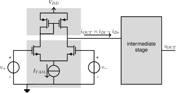
Like in chapter 5, conflicting requirements can be circumvented by using multiple amplification stages55 . Some stages that can be used in opamps are identical to circuits in chapter 5, while others are specifically catered to their specific task in the opamp. The general construction of an opamp is shown in Figure 8.1: an input circuit that satisfies all the input requirements, an output stage that does the same for the output and something in between that completes the total behaviour.
First of all, the input stage will be discussed in §8.2. This circuit is unlike any other that has been dealt with in this book so far. Input stages operate on a differential input voltage and usually have a differential output current, that is often converted to a single-ended current to be processed further. This (possible) conversion is dealt with in §8.3.
The output current of the input stage is amplified and converted into a voltage in an intermediate stage; these stages are discussed in §8.4. To correctly operate an external load, dedicated output stages are often needed; these are discussed in §8.5. Finally, bandwidth limitations are dealt with in §8.6.1.
The input stage of an opamp must meet a number of requirements, which follow from the practical applications of an opamp. The input stage:
must operate on a (typically small) differential input voltage
that can be either positive or negative and that can be at DC or that can be a fluctuating signal.
should be insensitive for the common-mode part, or average pat, of the input signal
Being insensitive means that for example for input voltages the response of the opamp must be the same as for input voltages .
From the first requirement, it follows that the circuits in chapter 5 cannot be used as input stages for an opamp: they do operate on small signal variations, but these small variation must be about a (non-zero) bias voltage. The left hand side circuit in Figure 8.2 illustrates this problem: here the differential input voltage is directly applied to the NPN’s base and emitter terminals which results in extremely poor biasing and hence in extremely poor transconducatance for very small , see also §3.1. Using an MOS transistor or an PNPs instead of the NPN does not solve the issue.
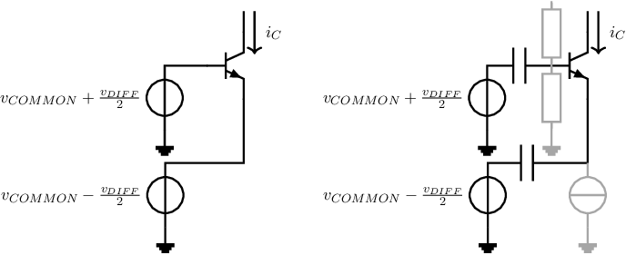
The problem sketched above can be solved using decoupling capacitors as was done in chapters 4 and 5: in that case, the input voltage does not need to be close to the bias level. For example, we might bias and drive the transistor using the circuit on the right hand side in Figure 8.2. Here the biasing circuitry is shown in grey. However, these types of circuits have a low gain for low frequencies — actually zero for DC — which is not acceptable for opamps.
As shown before, a single transistor circuit cannot implement a stage that processes arbitrary differential signals — from DC to high frequencies — symmetrically. From the definitions of “differential” and “common”:
it can be seen that the differential input signal to amplify, is symmetrical around the common part of the input signal. To properly (symmetrically) operate on something that is symmetrical, one usually needs something that is also symmetrical. A single transistor circuit, sadly, is not.
There are multiple ways to create a symmetrical circuit, that can operate on small differential input voltages, and that outputs a symmetrical output current as a (symmetrical) function of the input voltage. This book will deal with a few relatively simple circuits; more complex circuits are typically variations on these basic circuits.
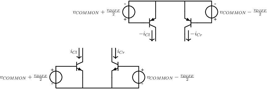
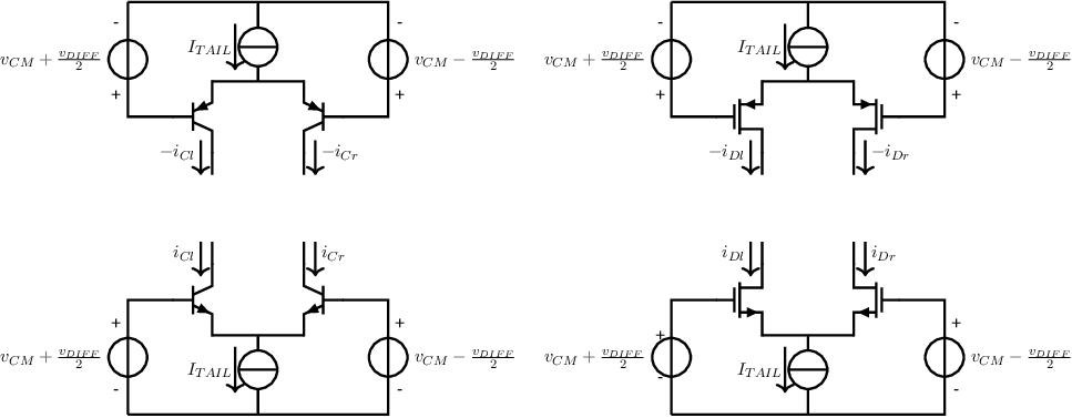
Assuming the use of asymmetrical components (like MOS transistors, BJTs or any other electrically amplifying component), it is possible to realize symmetric functionality with 2 of those components. From the requirements for symmetry and the use of transistors, it follows immediately that (in the case of a BJT):
A possible implementation of this is given in Figure 8.3, shown with NPNs and PNPs.
The transfer function from differential input voltage to differential output current for the NPN version is
Figure 8.4 shows the relation in (8.1) for four levels of . The is increased with — each time — 60 mV going from curve (a) to (b) to (c) and to (d). Note that the transfer function heavily depends on the .
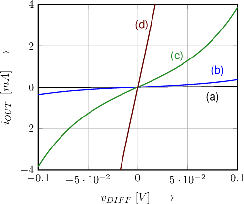
This circuit does have a some (related) problematic properties. Firstly, the supply current in the circuit is strongly dependent on , which is obvious from (8.1) if we set :
This strong dependency of the current on is also the cause for the second problem of this circuit: the — small signal and large signal — transfer function depends strongly (exponentially) on :
It can be concluded that the circuit in Figure 8.3 actually is a differential stage: it outputs a differential current that is a reasonably nice function of the differential input voltage. However, it does have a number of issues that follow from its strong dependency on the common mode level of the input voltage.
The MOS equivalents of the circuits in Figure 8.3 have pretty much the same behaviour as the BJT versions that are discussed: these, too, have a strong dependency on the common input signal. Interestingly, assuming square law operation for the MOS transistors, the MOS versions have an output current that is exactly proportional to the differential input voltage.
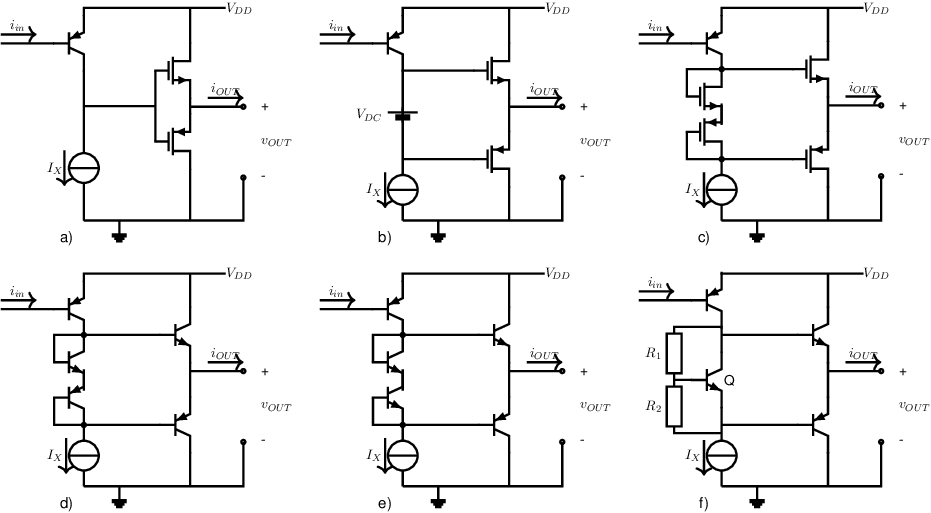
The circuit shown in Figure 8.3 would suffice as an input stage, if we make sure that the (bias) currents through both transistors are independent on . The usual way to make a current independent on a voltage is to use a current source. This results in the following input stages (which are obviously all equivalent) that are essentially the ones in Figure 8.3 biased from a so-called tail current source at their source or emitter nodes
In this book, the large signal transfer function is pretty much never used. A few relevant properties of this transfer function, like slope around and maximum output current, are presumed to be easily calculated.
The large signal transfer function of the differential pair of BJTs may be calculated as follows (for ideal NPNs, for PNPs the derivation is almost the same):
This shows that the large signal transfer function is both symmetrical and independent of . By taking the derivative of this transfer function the transconductance of the input stage (here around ) can be calculated: . Of course, you may also calculate that much more easily by using a small signal equivalent circuit.
Calculating the large signal transfer function of an input stage with MOS transistors requires a bit more effort than for the bipolar variants, because quadratic relations are harder than exponential ones. Assuming that the MOS transistors are in saturation:
This is a slightly dodgy equation, which can be simplified into a 2 order equation in . We could solve it using (for example) the abc formula, leading to e.g.
This is a true abomination, which even has a certain validity region, due to the square root in it... Luckily, you usually only need to know the extreme values and you only need to be able to calculate the small signal transfer.
For the 4 circuits given in Figure 8.5, the large signal transfer functions are ugly, complex and also not very relevant (which latter point is nice). When using these input stages in an opamp, only two situations usually occur56 :
Because the input stage is designed to operate on small (differential) signals, this type of circuit is usually called differential stage (or, in the case where 2 transistors are used: differential pair). Being symmetrical, their behaviour around the point of symmetry () is symmetrical. With small input signals, this translates into reasonably linear behaviour.
With large voltage differences , one of the transistors will conduct almost no current, and the other conducts almost all tail current. In other words: with large input signals, the differential output current will be .
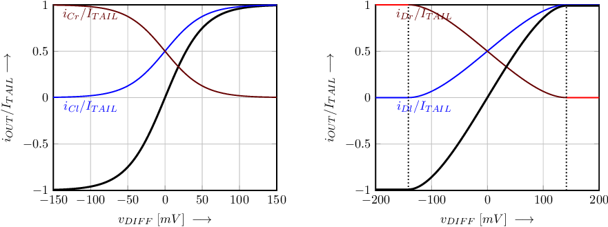
In Figure 8.6, the (large signal) transfer functions of a BJT differential pair and of a MOS differential pair are given. Both are S-shaped curves, which have as maximum and minimum. However, there are also differences between the large signal behaviour of BJT and the MOS versions:
The curves in Figure 8.6, also show that the currents through the individual transistors are scaled and shifted (by ) versions of the total output current. Note that this is a result of the symmetry in the circuit.
Differential pairs are used as input stages for opamps. For opamps that are used in linear (non-switching) applications, the input signal is usually very small, and the small signal behaviour of differential pairs is important. For two N-type differential pairs, both the circuit schematic and its small signal equivalent are given in Figure 8.7. These SSECs will be used to derive small signal properties of differential pairs.
Note that the MOS version of the small signal equivalent circuit has an apparent floating voltage node: only two voltage controlled current sources are connected to it. At first instance this configuration may seem strange, but the voltage dependency of the current sources make derivations surprisingly simple58 .
The most important property of a differential pair is its transconductance about . In the case of the small signal equivalent circuit for the BJT differential pair in Figure 8.7, a derivation for that explicitly leverages symmetry can be:
A different derivation — without explicitly using symmetry — can be:
When put into words, bottom line, the transconductance of a BJT differential pair is equal to the transconductance of the individual transistors in the pair. It can be derived that this has to be the case in these kinds of symmetric circuits. As direct consequence it follows that : the small signal collector currents do not flow through the (small-signal) base-emitter resistances due to symmetry.
The input impedance of a differential pair with input voltages around V, can be derived in a way similar to the one discussed above:
Due to symmetry in the differential pair, the small signal base current have the same (absolute) values but opposing signs: . Effectively this means that the input impedance equals the two base resistances in series.
For small signal transfer functions, a MOS transistor behaves identically to a BJT with an infinite current gain factor . Then, the transconductance of a MOS differential pair follows directly from (8.4) by letting : .
From (8.5) and substituting , it follows that . Note that the input impedance — if the MOS transistors’ is not neglected — is .
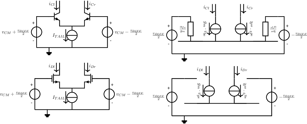
In the previous subsections, the (ideal) small signal behaviour of differential pairs was derived. These differential pairs assume an ideal current source that is usually called a tail current source. In actual circuits, a (tail) current source is made using, for example, a MOS transistor with a constant (see §5.3.2), or a resistor. In the figure below, an NMOS differential pair with a non-ideal tail current source is shown, together with the corresponding small signal equivalent circuit. Resistor models the output resistance of the current source implemented by the right hand side NMOS in the current mirror in the figure.

The transconductance of the differential pair is easily calculated from the small signal equivalent circuit. The resulting expression is (again):
where the transconductance of transistors depends on the bias current of the transistors, and therefore dependent on the total tail current. In contrast to when using an ideal tail current source, now the tail current is dependent on the common input signal, due to the presence of a finite .
The effect of and the common input signal on the output current is easily calculated for V. On grounds of symmetry in the circuit and in the input signals, the drain currents of the transistors in the differential pair are identical. The output current is therefore equal to 0. If the circuit is asymmetrical for any reason, for example due to unequal transistors in the pair or because , there is also an output current component resulting from .
In §8.2, input stages were discussed, and these input stages are usually differential pairs as shown in Figure 8.5, or variations on them. For these kinds of differential stages, the transfer functions were calculated in multiple ways, always assuming that the output signal is : a differential output current.
These differential output currents are then (in an arbitrary order) amplified and converted to a voltage. Because the differential output current consists of 2 currents, and usually the output signal of the opamp is 1 voltage, somewhere there has to be a transition from differential to “single-ended”. This is the subject of this subsection, assuming a MOS differential pair as an vehicle. Figure 8.8 shows an NMOS differential pair with several forms of conversion from differential current to single current.
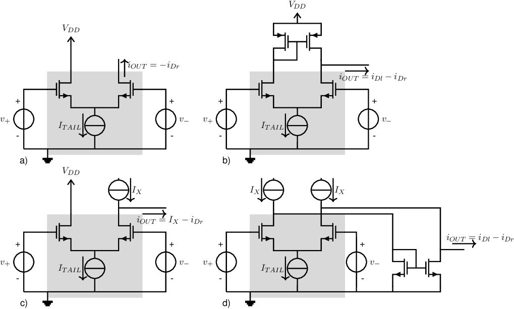
To easily recognize the various parts of the circuits, the NMOS differential pairs are drawn over a grey background. The four example circuit implementations are briefly discussed below.
The simplest way to make a single-ended current from a differential current, is to simply throw away one of the differential current components. This has been done in the simplest possible way in Figure 8.8a. For an ideal differential pair, the output current (note the direction of the output current) for small input volages is
where is the transconductance of the transistors in the differential pair. The small signal transconductance of the total circuit in Figure 8.8a is hence
A possible disadvantage of the circuit in Figure 8.8a, is that the output signal contains a fairly large DC current component — — which may lead to problems in subsequent intermediate stages. A solution for that is given in Figure 8.8c: throwing away half of the differential signal, and then compensating for the by adding that same value from another DC current source . That leads to the following output signal:
|
| (8.6) |
To use the differential output current of a differential pair, the two drain currents and can be subtracted from each other. In this case, the common part in the currents — — cancel and the differential currents add.
Adding currents is easy, as is reversing a current’s direction (using the current mirror in §5.3.3). Consequently, subtracting currents is also easy: first invert one component with a current mirror, and then add both currents. A corresponding circuit is shown in Figure 8.8b. The output current is (assuming an ideal differential pair and an ideal current mirror):
Note that for proper operation, all transistors in the circuit schematic must operate as intended. Usually this implies that all transistors should operate in (strong inversion) saturation. Similar to the case with single-transistor amplifiers, this limits the
The input stage of an amplifier is usually a differential pair, which has a voltage input and a current as an output. The output signal of an opamp is in the voltage domain while the overall voltage gain of an opamp should be a large as possible. Therefore another amplification stage, which converts the current to a voltage and that preferably has a large transresistance () is needed. This is the function of the intermediate stage, which is dealt with below. Often (but not always), an output stage is required after the intermediate stage, in order to reduce the opamp’s output impedance. Those kinds of output stages are dealt with in §8.5.
The most important requirements for the intermediate stage are:
Like for the other stages, there are many possibilities for the intermediate stage. A few examples, increasing in complexity, will be discussed here. Assuming these basic configurations, variations on them are easier to understand and design.
The most simple implementation of a voltage to current converter is a resistor. If a resistor is used as an “intermediate stage”, the resulting opamp, using an input stage with an NMOS differential pair and a PMOS current mirror, is shown in Figure 8.10.
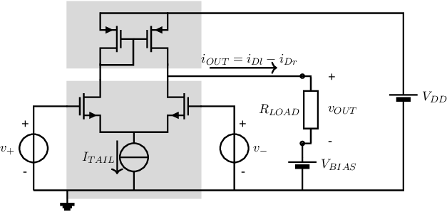
The DC voltage source with value is needed to keep and in saturation for small . The small signal output voltage of this circuit is
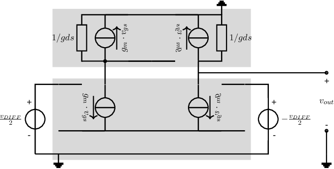
The resistance can be applied explicitly, or can consist of the (non ideal) finite output resistances of the MOS transistors. If only the output resistances of the transistors in the mirror are present, the small signal equivalent circuit of the schematic in Figure 8.10 is shown in Figure 8.11. The small signal output voltage, assuming a symmetric differential pair and current mirror, is then
If the output resistances of the transistors in the differential pair are also included, the result is similar. This is also reflected in the very similar (8.8) and (8.9).
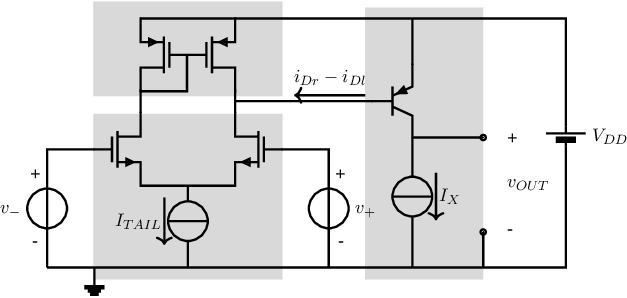
A somewhat more complex intermediate stage could consist of an active element as a load and extra gain stage. In this way, for example the circuit n Figure 8.12 may result. In this circuit, the current flowing from the combination of differential pair and current mirror is used to drive a PNP in a CEC configuration. Note that compared to Figure 8.10 the positive input and negative input swapped, due to the negative voltage gain of the CEC stage.
Performing calculations on this circuit can be done in several ways:
Below, the second option is assumed. As simplification, it is assumed that output conductances of all transistors can be neglected, and that the differential pair and mirror are symmetric. Then — without redrawing small signal equivalent circuits for the various parts of the circuit in Figure 8.12 — for the circuit bits in the three grey areas
the small signal transfer for the NMOS differential pair is
The transfer function of the PMOS current mirror is
For the combination of NMOS differential pair and PMOS current mirror, this leads to:
The intermediate stage consisting of a CEC converts its input current into an output voltage. There are several equivalent ways to calculate the transfer function. For example, you may calculate the (small signal) input voltage as a function of the input current which, together with the voltage gain, leads to the transfer function of the intermediate stage. For simplicity (of interpreting the result), an (combined) output resistance at the collector node equal to is assumed.
Note that the first equation assumes current gain, while the second one assumed conversion at the small signal base-emitter resistance and subsequent transconductance. Of course the bottom line results are identical.
Combining the transfer function of the three parts, and noting that (for simplicity reasons) the output impedances of the differential pair and of the current mirror are infinite, the overall small signal transfer function is
The various small signal parameters (of course) depend on the large signal bias conditions. Obviously, there are many more interesting things to derive from this circuit, like , . These are all useful, and it is also useful to derive these yourself.
Opamp circuits with more complex intermediate stages are also quite easy to examine, as long as the circuit is first subdivided in easy-to-analyze subcircuits. Figure 8.13 is an example of a slightly more complicated intermediate stage (together with a differential pair and current source). There are many ways to calculate the transfer function of this intermediate stage:
Note that in the first case, every stage (in the intermediate stage) is regarded as a voltage amplifier, while in the second case they are regarded as current amplifiers. This choice is arbitrary; when including the relations for input and output resistances, they yield identical results.
Assuming that the output resistance of all transistors is infinite, and assuming a load resistor , the small signal voltage gain of this circuit is
The first two terms of this expression are due to the non-unity (current) transfer of a bipolar current mirror. For large you the second term on the right hand side tends to 1 and may be ignored.
For the opamp circuits discussed so far, the output impedance is quite high. For the circuits in section 8.3, the output signal is in the current domain: therefore, the output impedance is high. The same thing basically holds for the intermediate stages discussed in §8.4.
For a lot of applications, the output impedance of opamp circuits should be (relative to the load) low. Leveraging negative feedback, the output impedance can be reduced by a factor compared to that in the open loop configuration, but even then the output impedance may be too high to properly drive a low ohmic load.
As solution, usually an extra (last) gain stage is used to lower the output impedance. Such output stages — having a high input impedance and a low output impedance and typically having a low voltage gain — is of course not a new concept: in section 5.2 this has been dealt with extensively.
The most important requirements for an output stage are:
In section 8.5.2, the first two requirements are dealt with. Afterwards, in section 8.5.6, some attention is paid to efficiency aspects of various types of output stages.
In section 5.1.7, various aspects of the 3 basic configurations using BJTs have been summarized. The summary for corresponding MOS variants is given in section 5.1.7. From the summaries, it is clear that especially the CCC — a.k.a. the emitter follower — and the CDC — a.k.a. the source follower — are good candidates for output stages: these circuits have a high input impedance and have a low output impedance. These circuits will first be examined for use as an output stage in opamp circuits.
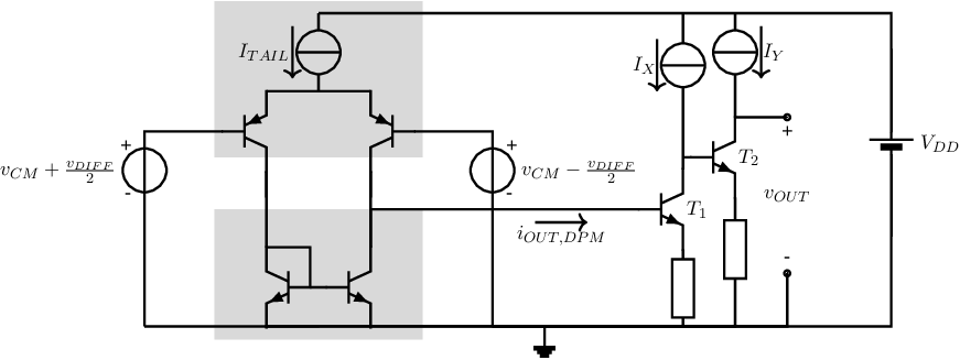
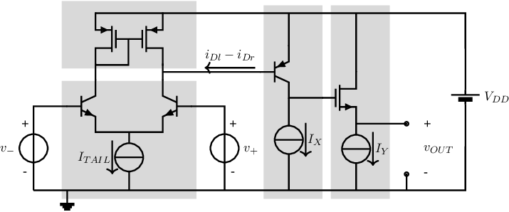
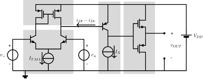
One of the most simple output stages for opamps is the source follower with tail current source; a schematic of such an opamp circuit is given in Figure 8.14. Note that in order to examine the entire opamp circuit, it has been subdivided into 4 parts: a differential pair, a current mirror, an intermediate stage and the CDC output stage. It is assumed that the output impedance of the pnp is and that there is not extrnal load attached to this opamp.
The small signal gain of this opamp can be calculated by e.g. determining and multiplying the small signal transfer functions of each subcircuit. Note that the effects of input and output impedances should be properly included! The result, for the circuit in Figure 8.14, is:
The small signal output resistance of the opamp circuit in Figure 8.14 can be calculated in multiple ways. For the derivation below, a small signal voltage source drives the output port; the output impedance is then calculated as . Note that for this approach, the only independent source is the one driving the output port; all other independent sources have to be set to 0.
Inspection of the circuit in Figure 8.14 shows that the small signal . Consequently the small signal collector current of the pnp is also 0. Therefore, the small signal circuit equivalent circuit — to calculate assuming driving the output node — is the one on the right hand side in Figure 8.15.
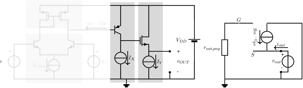
It can be derived that for finite , the output resistance of the opamp circuit in Figure 8.15 is
while for
Quite similar results follow when using a PMOS CDC or if a NPN or PNP CCC is assumed as output stage. Be aware that the output impedance is purely a small signal output impedance. At significant (relative to the bias current) output current fluctuation, the (then locally defined) small signal output impedance may change significantly.
Non-small signal excitation example
The output impedance as derived above is only valid for small signal excursions where the current in the
NMOS transistor does not varies significantly. Furthermore, it is the output resistance of the opamp itself, not
that of a circuit including the opamp in a feedback configuration. Because the output stage op the opamp is
meant to drive relatively low-ohmic loads at significant voltage excursions, the small signal approximation
may not hold.
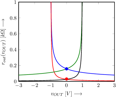
Let’s assume that the opamp in Figure 8.15 has a high voltage gain and that it is used in unity-gain mode. In this mode, the small signal voltage gain is
which closed loop signal transfer is close to 1 as long as the gain of the opamp is high. This high gain condition depends — among other — on the gain and output impedance of the output stage of the opamp. Now, assuming
the drain current in the NMOS transistor is the sum of the bias current and the signal current . The output resistance of the CDC — and that of the opamp — across the excursion is then
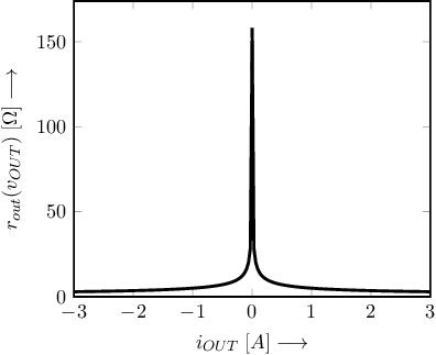
The figure below shows in red the drain current in the NMOS transistor as a function of , for the aforementioned conditions. In blue is the (local) as a function of the output voltage. For small signals around the bias point, the drain current is close to and the output impedance of the output stage is about ; this point is marked by the blue dot in the graph.
Note that for , the drain current is doubled with respect to , resulting in a lower output resistance of the output stage of the opamp. Towards higher output voltages, the (local) output resistance decreases.
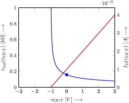
Towards negative output voltages, the drain current of the NMOS transistor decreases, and is zero at . There, the output resistance goes to infinity. The output stage does not work properly for excursions above .
Going to PMOS, PNP or NPN output stages with the same bias current level (and for the PMOS the same ) yields similar curves. Note that the BJT-versions have lower output resistances, and note that N-versions and P-versions are merely mirrored in the y-axis.
From this, two methods arise to make sure the output resistance remains low for relatively large — positive and negative — output currents:
As shown in §8.5.2, basic output stage that have relatively low output impedance (e.g. CDC or CCC stages) can be used as proper opamp output stage, as long as the current in the transistors in that stage remains sufficiently high for any output voltage. To be able to drive low ohmic loads this then would require sufficiently large bias currents. Noting that the output current can either increase the current in the transistor (in CCC or CDC) or decrease it, depending on its direction, a more power efficient way to make output stages can be deviced. A first implementation for this is given below, combining two complementary CDC circuits:
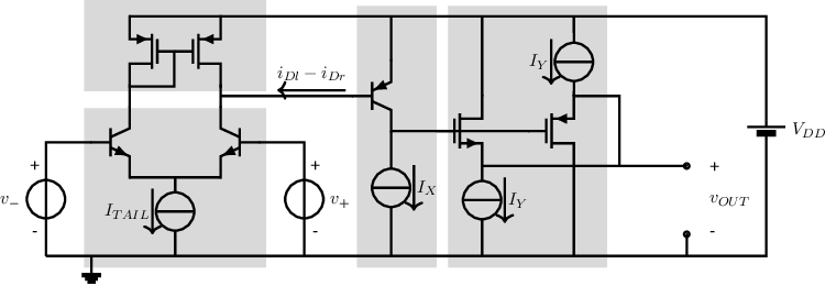
Note that the output stage of the opamp schematic is basically an NMOS and PMOS CDC in parallel. Here, the two current sources are in series between the supply nodes. Assuming that they have the same value, these current sources only sink current and have no use whatsoever for the circuit. Consequently, these can be deleted, which allows to redraw the circuit schematic into:
A graph showing the output stage’s transistors’ current as a function of the opamp output current is shown below. The red curve shows the drain current of the NMOS transistor, whereas the red curve corresponds to the output stage’s PMOS transistor drain current.
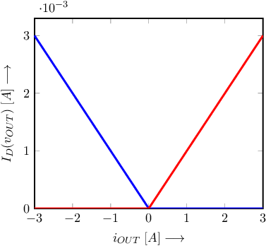
This dependency of the output transistors’ drain current on the opamp output current yields the following graph for the output resistance of the opamp, as a function of the opamp output current. For this circuit configuration, either the NMOS transistor or the PMOS transistor is “on” and hence determines the output resistance.
At (close) to zero output current the output resistance of the opamp is high. Note again that when using the opamp in a feedback configuration, the output resistance of that total circuit configuration is typically that of the opamp, lowered by (1+) the loop gain.
Similar to the situation with single transistor amplifiers in e.g. chapter 5.1, an lower output resistance lower than some value for any output current level can be insured by making sure that the current in the output stage transistors is always higher than some specific value(s). Some examples are given in the next subsection, that all aim at making sure that at least one of the output stage transistors sees a sufficiently large drain current. Again similar to what was done in chapters 3-5.1 this requires a bias (quiescent) for bias output stage transistors.
To ensure that the current in at least one of the output stage transistors is sufficiently high for proper operation of the output stage, typically a sort of “floating DC voltage source” is implemented between the gates (or bases) of these.
In actual circuits, the floating DC voltage source is implemented with electronic components. Because the current through the output stage is quite dependent on the value of and of (temperature dependent) properties of the transistor, the DC source is often realized with transistors that behave similarly to the output stage transistors. Below, a few output stages, with different realizations for , and with an intermediate amplification stage using a (PNP) common-emitter circuit are shown.
The realization in a) is copied from the previous circuit schematic in this subsection, having zero bias current in the output stage transistors (with zero signal excursion). The realization in b) uses an ideal floating voltage source.
Figures c) to f) in the figure below are straightforward implementations of the DC source using compensation for temperature and production offsets. Here it is assumed that the transistor(s) that replace the floating voltage source match the output transistors, up to a scaling factor. Then the output transistors’ bias current is a scaled version of .
A nice implementation, where with can be realized with a BJT, is shown in f). If, for simplicity, we neglect the base current through Q, it is easily derived that , with .
The large signal signal transfer and large-signal-dependent small signal output impedances can be derived for the presented output stages. As these are large signal derivations, they need to include the non-linear characteristics of the transistors which is harder than getting small signal behavior about a bias setting. Full derivations are outside the scope of this book, and usually not required. Deriving the small signal transfer and impedances in three situations is usually sufficient; these situations are for zero output current, maximum negative and maximum positive output current.
Output stages of opamps59 are used on relatively low impedance loads. To do this correctly, relatively high output currents are needed, see for example §8.5.4, which can cause high power consumption in the output stage. In this subsection, the power efficiency of various output stages will be discussed.
The simplest output stages of opamps are usually emitter follower or source follower circuits, see §8.5.2. An example of such a circuit is given in Figure 8.14; the (large signal) output current for these types of circuits is:
If we assume that the output current is symmetrical, the highest possible harmonic output current60 is:
The output power and the power delivered by the supply are:
The maximum value of the output voltage is determined by the supply voltage: if the output signal only just fits into the supply voltage, it holds that . The maximum power efficiency of these kinds of output stages, therefore, is:
From (8.10), it follows that the maximum power efficiency of these kinds of circuits is only 25%. Note that this efficiency number can only be reached if the output signal perfectly fits into the supply voltage; for lower signal magnitudes the efficiency is lower. This low efficiency occurs in all amplifiers where the output signal is made, as described before, with only a single transistor. These types of amplifiers are the oldest and simplest in existence, and are denoted as class A. Strictly speaking, class A stands for an amplifier where the output transistor(s) drive the load for the entire duration of the signal.
In §8.5.4, a few less simple output stages were discussed, which can deliver reasonably large output currents using a bias current lower than the maximum output current. This was accomplished by using two transistors, each mainly responsible for a different part of the output signal. A number of implementations for this are shown in §8.5.4.
If, for simplicity, it is assumed that both transistors make up exactly half of the output sine, the output power and the supply power are again easily calculated:
Again, maximum power efficiency is reached at the maximum voltage magnitude:
Whereas with class A amplifiers, the maximum efficiency is 25%, that number for these amplifiers is % which number is reached at maximum signal excusions. Amplifiers where one of two (quasi) symmetrical parts are driving for exactly 50% of the output signal are called class B amplifiers.
In class B output stages, the two parts of the output stage drive exactly 50% of the output signal. This means that transistors in the other part of the output stage are “off” for 50% of the signal. In §8.5.4, a number of disadvantages of pure class B output stages are listed: among others the output resistance can be high at specific operating conditions. Another disadvantage (outside the scope of this reader) is that transistors are very slow at low current levels. Solving the issues that come with having transistors “off” is simple: ensuring an overlapping “on” range of both parts of the output stage. The resulting output stage is not class A, and not class B, but something in between: a class AB output stage. The maximum power efficiency of class AB, therefore, is:
A different type of output stage is the class D stage. Where class A, AB and B work pretty “neatly”, a class D amplifier does not. In a class D amplifier the output switches between two discrete values, where the actual output signal is the resulting quasi-DC component which is something like the short-term average of the switched signal, where all higher components are filtered out.
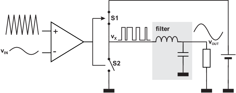
If, for the basic schematic in Figure 8.16 the switching frequency (frequency of the triangle) is much higher than the signal frequency, the signal can be regarded as quasi-DC. In the system in Figure 8.16 the “on” times of switches S1 and S2 are linearly dependent on the input signal level, as is then the quasi-DC component of . After filtering out the switching frequency and its harmonics, is an amplified version of the input signal .
The very nice property of this type of amplifier is that the switches are either “on” with a voltage drop of (ideally) 0V, or “off” with (ideally) no current in the switch. Consequently the power efficiency of an ideal class D amplifier is 100%. Dissipation in the control circuitry and switching losses, as well as non-ideal filtering reduces the power efficiency to typically around 90%.
There are many more types of output stages than those discussed just now; a large part of the alphabet has been reserved for them. The class C amplifier is essentially a class A or class B amplifier, where only a part of the input signal is actually amplified. It yields distorted output signals, similar to those in Figure 3.1, at a high power efficiency. Class E and class F amplifiers are resonant amplifiers meant to efficiency amplify narrow band signals such as radio frequency (RF) signals in power amplifiers in transmitters. Class G and H are variations on the ones mentioned before, but using a variable supply voltage.
The combination of resistances and capacitances usually leads to bandwidth limitations. In actual transistors, many capacitances are present. In bipolar transistors these are mainly the (parasitic, unwanted) junction capacitances across the base-emitter and base-collector junctions. In MOS transistors some capacitances are fundamental while others are just parasitic, usually both are unwanted and also assumed to be parasitic. In previous chapters, parasitic capacitances were all neglected which may be acceptable at low signal frequencies. At higher frequencies they however cannot be neglected. In §8.6.1, the effect of parasitic capacitances will be analyzed and “solved” for small signals. Then, in §8.6.2, the effect of limited bandwidth on large signal behaviour will be discussed.
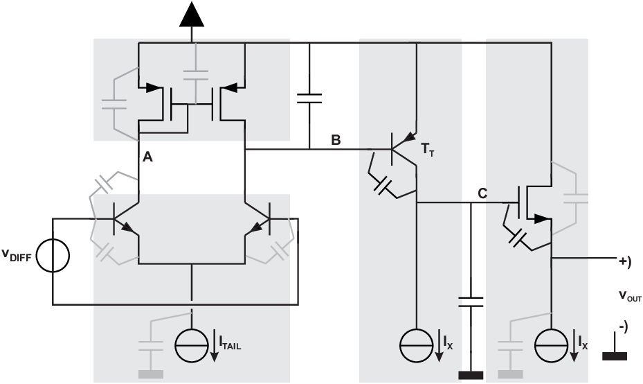
If the parasitic components of transistors are explicitly included in an opamp circuit, you may get something like Figure 8.17. That circuit comprises 6 transistors and 3 current sources (that may again be composed of transistors). This yields already a circuit with 16 capacitors, which makes analyses quite complex.
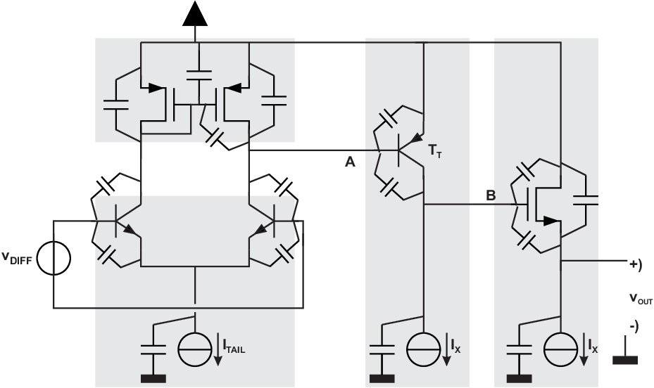
To analyze the behavior of this circuit, circuit can be rewritten into a much more easy-to-read form. For this, many capacitances can be replaced by single capacitances. Because this circuit has 3 internal nodes and one (not low-ohmically driven) output node there is only a low number of capacitances required that are equivalent to the 16 shown in the figure. As next step to reduce the complexity of analysis it is useful to realize that usually one frequency limitation is the worst (dominant) and that others then are not that relevant. It can be argued that:
In the given circuit — and generally, when dealing with parasitic capacitances — parasitic capacitances usually dominantly introduce low-pass characteristics61 . For a low pass behavior due to the impedance at a node, the associated cut off frequency is from which it follows that (almost) all parasitic capacitances that are between 2 low ohmic nodes, are not very relevant. The schematic of Figure 8.17 can then be reduced to that in Figure 8.18 allowing (relatively) easy calculation of small signal properties.
Bandwidth limitations have different effects on a large or small signal level. For small signals, it just shows as some kind of low pass or high pass filtering effects, which are linear effects. For large signals, however, it can cause nonlinear effects. A description is in this paragraph, using a (generally valid) example.
Assuming, for simplicity, an amplifier with dominant first order behaviour, the open loop transfer function can be given by the following relation. In this, linear behavior is assumed which allows using the frequency-domain relation.
If this amplifier is used in a configuration with negative feedback — as is often true for opamps in linear applications — the input signal of the opamp is ideally
Equation (8.13) still assumes linear behaviour of the amplifier. Having e.g. an differential pair as input circuit for an opamp, the gain is both frequency and input voltage magnitude dependent. Whereas for small signals the input voltage dependency may be neglected, for large signals this is certainly not the case. For relatively large input voltages the output current of a differential pair is limited to the value of its tail current source; in that situation the small signal gain has dropped to 0 and effectively loop gain also dropped to zero. Modelling (assuming) this as the actual limit of linear-ish behavior in a feedback system, then for an opamp similar to the one in Fig. 8.18:
leading to a maximum rate at which voltage at node B can change:
In this equation is the total capacitance at node B. This is composed of the capacitance across the base-emitter of and of the capacitance at node B due to the so-called Miller capacitor across base-collector. Assuming a small signal voltage gain of equal to then the total capacitance at node B equals . The maximum rate at which the output voltage of the opamp can change is
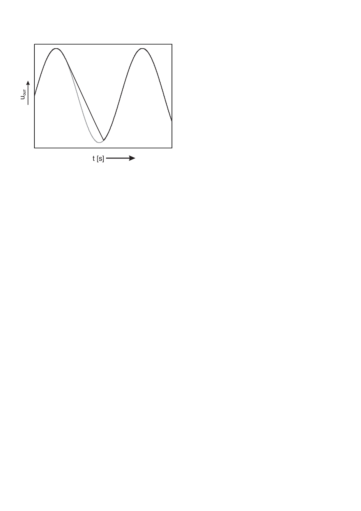
This maximum slope of the output voltage is called the slew rate (SR). An amplifier running into these kinds of slew rate limitations is usually said to be “slewing”.
Let’s assume that a sinusoidal signal must be amplified, using an amplifier with a limited slew rate. Then the signal frequency in combination with signal magnitude determine the maximum rate at which the signal changes in time, . Assuming an amplifier with a single sidedly limited (too low) slew rate,
For an output sine , the required slew rate for a neat amplification is . If the required SR is higher than the actual slew rate of the amplifier, a part of the sine wave will see distortion, see the figure below.