Chapter 9 covered harmonic oscillators with a low quality factor. As shown in (9.1), a low Q corresponds to a high loss of energy per oscillation period. In harmonic oscillators the oscillation amplitude is constant which implies that there has to be some active component in the oscillator to compensate for this loss of energy per oscillation period. For the oscillators in §9.3, this loss of energy is compensated for by circuits like ideal(ized) voltage amplifiers that can be implemented with e.g. opamps with a suitable (negative) feedback to set a specific voltage gain .
Creating low Q oscillators becomes increasingly difficult for higher frequencies because amplifiers are harder to design at higher frequencies while the power that must be compensated for () increases with increasing frequencies. The current section covers oscillators with a high quality factor. Sections 10.1, 10.3 and 10.4 cover high Q oscillators with amplifiers consisting of just one transistor; harmonic oscillators that require more than just one transistor are treated in section 10.5 while a number of examples of the latter are shown in 10.6.
To create high Q oscillators, the dissipated energy per oscillation period must be minimized. A first step is the omission of any explicit power dissipating components (resistors) from the oscillator. Consequently, high-Q oscillators are mainly using inductors and capacitors, with an amplifier circuit — that preferably have a very low impact on the oscillation frequency and power dissipation — to compensate for the energy loss per period.
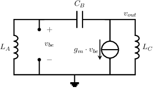
The circuit for high Q oscillators typically uses a mixture of capacitors and inductors. In this chapter, single transistor amplifiers are assumed since op-amps are less suited for high frequency operation. Figure 10.1 shows a generic oscillator topology where the amplifier is implemented as a (non-degenerated) common emitter or common source amplifier. As shown in chapter 4, these have a negative voltage gain .
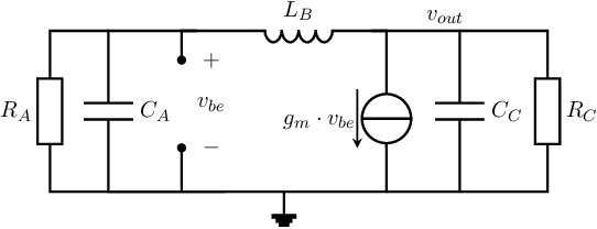
The small-signal equivalent circuit of both amplifier circuits in 10.1 is depicted in Figure 10.2:
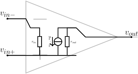
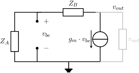
The input resistance of the (small signal equivalent of the) amplifier in Figure 10.2 is finite due to both the transistor’s input resistance (for a BJT) and due to the required bias circuitry. The amplifier’s output resistance is due to the collector or drain resistance, and due to the output resistance of the transistor. Ideally both and are high ohmic to dissipate a minimum of energy.
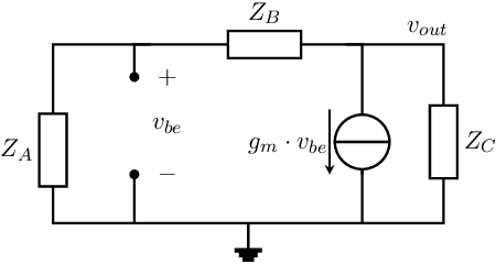
For a single transistor amplifier circuit in an common emitter or source configuration, the small-signal equivalent of this amplifier with feedback via impedances and is shown in Figure 10.3.
The circuit oscillates harmonically if the total loop gain equals 1 for just one finite and non-zero frequency. Deriving the loop gain can be done as introduced in section 9.4:
In the configuration as shown in Figure 10.3, the loop can safely be opened in the exact same way as in section 9.4: inside an ideal two port component that implements a controlled source. In the above figure, that opening of the loop would then be inside the SSEC of the BJT. Doing so, the actual is mathematically disconnected from the in the source that delivers . For now let’s denote the (opened loop) input voltage of the loop — that hence yields a current — resulting in an (opened loop) output voltage and a loop gain
For a negligible (e.g. very high ohmic) then
For oscillation, the loop gain in (10.1) must equal 1 for one finite and non-zero frequency. Because the transconductance of a transistor is real and positive, this would require a negative resistance for . Conventional passive components cannot perform such a function65 .
Looking at Figure 10.3 more closely, and analyzing it together with (10.1), a number of interesting conclusions follow:
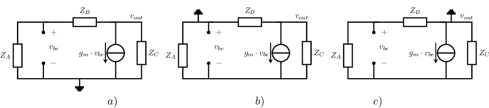
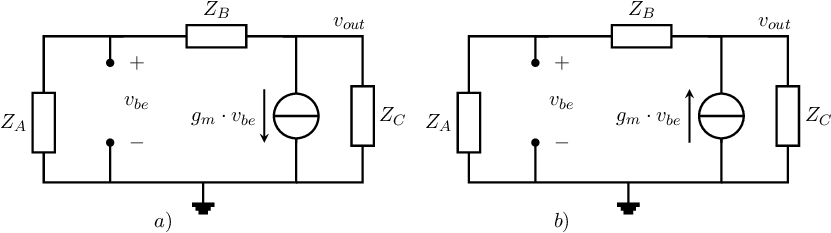
To satisfy the oscillation condition with the given circuit, we have to “rotate” the feedback voltage (vector) within the complex plane. In other words: we have to implement extra phase shift in order to be able to get harmonic oscillation. The simplest method for implementing extra phase shift is by adding an impedance parallel to , as shown in Figure 10.4. Note that this is also the most generic feedback configuration wrapped around a single (3-terminal) transistor.
The loop gain for the circuit of Figure 10.4 is easily obtained by cutting the loop inside the (ideal, two port) voltage controlled current source. Doing so and denoting the voltage that drives the voltage controlled current source and neglecting 66 this yields
From this, it follows that the oscillation condition for this type of circuit configuration can be written as
|
| (10.2) |
This condition can be satisfied in various ways, each leading to different implementations. for a high-Q oscillator using a single CEC amplifier.
For the circuit configuration in Figure 10.4, the oscillation condition can be written as (10.2):
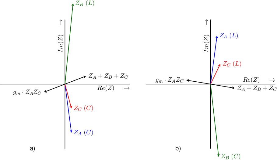
This condition can be satisfied in a number of ways which is demonstrated below. For this, first a few observations are explicitly stated for simplification reasons:
From the above enumeration, we find the following possibilities for :
Combining all this immediately reveals that that the vector will always be in the first or fourth quadrant. To satisfy (10.2), the vector must also be in the first or fourth quadrant. Since is positive and real this can only be realized if and are reactive components of the same type (both inductive or both capacitive). To satisfy 10.2, for a finite non-zero , a suitable and a suitable are needed. The vector diagrams of both implementations are given in Figure 10.5a and b67 .
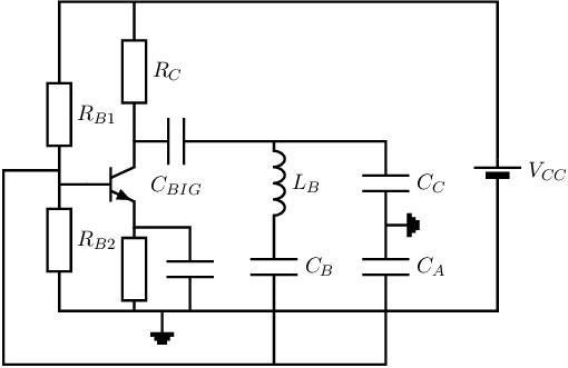
A number of single transistor oscillator types is listed in the table below; these all satisfy (10.2); also their (ideal oscillation (radian) frequency is listed.The various implementations are named after their inventors: Clapp, Colpitts, Hartley, Meacham, Butler, Miller, Seiler and Pierce. Few people actually know who invented which, but the first three are displayed in table below along with the corresponding (simplified) SSECs, assuming a common emitter amplifier stage.
| name | ssec | ||||||||||
|
|
|
|
| |
||||||
|
|
|
|
| |
||||||
|
|
|
|
| |
||||||
To determine the loop gain, the loop has to be opened somewhere, after which a(n harmonic) signal needs to be applied and the response to that by the (opened) loop is to be derived. There are multiple valid methods available for determining the loop gain:
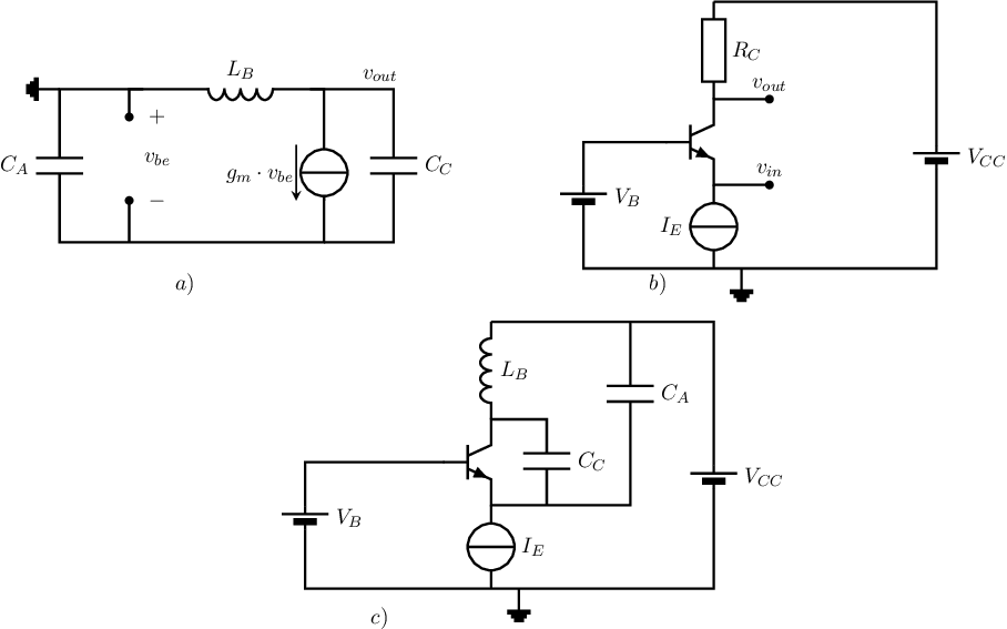
Figure 10.6a shows a basic configuration for a single transistor oscillator with impedances , and . In section 9.4, it was explained that the safest way to cut a loop to be able to derive the loop gain is cutting it in the middle of an ideal amplifier. In that way, no impedance level is changed due to opening the loop and including a signal source for analysis purposes. Only then derived expressions are correct. Similarly, in section 10.1 it was stated that in single transistor oscillators it is safe to open the loop inside a (small signal equivalent of a) transistor, in the middle of the voltage controlled current source as shown below.
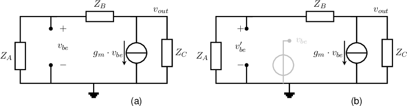
Opening the loop at a “regular” node risks changing either the source impedance, or the load impedance, or both. Similar to the case with low-Q oscillators, having a wrong impedance somewhere for derivation purposes only, yields incorrectly derivations. Using transistors, opening a loop inside the transistor as shown in Figure 10.6b does not change any impedance level: it is a purely mathematical trick to open the loop without changing any impedance level! Therefore, this is the method of choice to (mathematically safely) open the loop to properly derive loop gain. The loop is (mathematically) closed by setting .
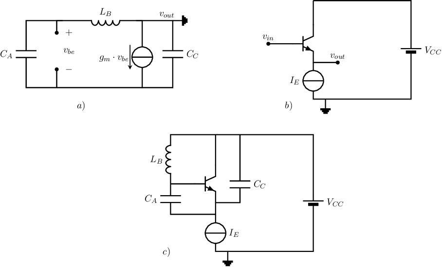
The previous section presented a general derivation for harmonic oscillators assuming a single common emitter based amplifier stage . It may be clear that its MOS equivalent — the harmonic oscillator with a gain stage in a common source configuration – is very similar. The small signal equivalent of the CEC-based harmonic oscillator is again shown in Figure 10.7a. Another option would be to assume one of the other single transistor amplifier configurations as gain stage in the harmonic oscillator. This can be e.g. a common gate, common base, common collector or common drain amplifier. The corresponding small signal equivalents (for BJTs) are shown in Figure 10.7b) and c). Note that in a small signal equivalent circuit, the “only” difference between all configurations is which node is actually assigned to be (virtual) ground.
Because mathematics really does not care what you or I assign or call ground, the corresponding oscillation condition for all of the configurations in Figure 10.7 is also given by (10.2). Consequently we can create the exact same oscillator types using
| name | |||
| Colpitts | C | L | C |
| Clapp | C | L+C | C |
| Hartley | L | C | L |
The actual circuit implementation of harmonic oscillators using single transistor stages with in CBC, CCC, CGC and CDC configurations are different for harmonic oscillator circuits using a common emitter or common source configuration based amplifier stage. Examples of this are shown in §10.4.
This section presents a number of high-Q harmonic oscillators using a single-transistor amplifier. In this section a BJT is assumed; extending the syntheses and circuits towards single MOS transistor oscillators is straight forward.
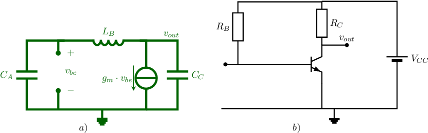
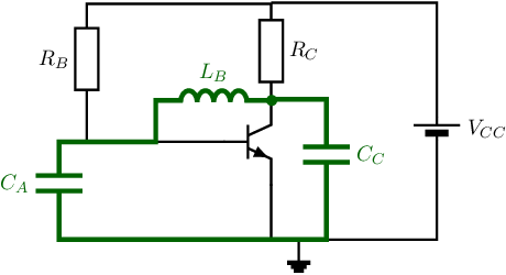
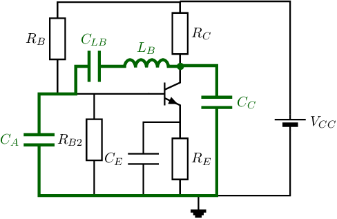
As example, a Colpitts oscillator with a common emitter amplifier is synthesized. For this, we start at the SSEC of an ideal Colpitts oscillator as shown in the figure below (subfigure a) and the CEC shown in below in subfigure b). Note that for the amplifier, a bare minimum voltage amplifier is used: only one resistor to bias the BJT, no emitter degeneration and no coupling capacitors at the input and output terminals.
To synthesize the Colpitts oscillator with common emitter amplifier,
A straight forward merge of the circuits yields the circuit schematic shown below. The Colpitts part is shown in bold/green for illustration purposes. The next step is to ensure proper operation of the combination of both the amplifier now the Colpitts configuration is merged with it.
Derivation for oscillation (signal)
For single transistor oscillators the loop gain was derived to be
|
| (10.3) |
where for this specific circuit implementation the actual , and follow from a SSEC:
Plugging these into (10.3) and solving to get a real valued yields the oscillation (radian) frequency. It is a nice exercise to verify that this yields
The required amplifier gain (either in transconductance or in voltage gain ) is a quite nasty equation that can easily obtained by equating to 1. The equation are much easier to handle (shorter) if
is — as a good approximation — capacitive which requires , yielding
or is — as a good approximation — capacitive which is satisfied if . Then
Derivation for biasing/amplification
The required value for transconductance as derived above must be ensured by proper biasing of the common
emitter amplifier in the total schematic. Note that no decoupling capacitances are required for capacitors
and
for biasing
purposes. Inductor
however shorts the base and collector at DC. A DC-equivalent of the synthesized circuit schematic of the Colpitts
oscillators is:
From this, it can readily be derived that the BJT’s bias current and transconductance are
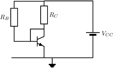
With the circuit schematic in section §10.4.1, the base and collector are at the same DC voltage level. Also, this circuit does not include bias current stabilizing feedback mechanisms such as emitter degeneration (with or without shunt capacitor) nor a high-ohmic resistor that sets the base current. To implement this, the DC-short between base and emitter must be removed. This can be done in the same way as was done in e.g. chapter 5: using a capacitor to decouple DC levels while passing actual signals.
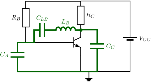
One example is shown below Note that for signals (the oscillation signal) this circuit is identical to the circuit in section §10.4.1 while this circuit allows bias stabilizing feedback via and .
Implementing bias stabilization via only emitter degeneration can be done as shown below. Note that bias current (stabilizing) feedback via and via can be added when omitting .
Many other variants of Colpitts oscillators with CEC amplifiers can be constructed. Noting that the ideal (SEC of a) Colpitts oscillator only includes 3 reactances and a voltage controlled current source (the ), one option can be to avoid having . To set a proper bias point, still a proper must be set. This can be done using a current source or using a high values inductor instead of . It may be clear that using a CEC in a Colpitts oscillator is not a requirement: also other types of amplifiers can be used; this is the subject of the next subsection.
In the previous subsection, some variants of Colpitts oscillators using a single NPN in CEC configuration were shown. It may be clear that Colpitts oscillators in CEC with PNPs are similar, and that implementations with NMOS or PMOS transistors in CSC configuration are also quite similar. In this subsection, Colpitts oscillators with single NPN amplifier stages in CBC and CCC configuration are worked out a little.
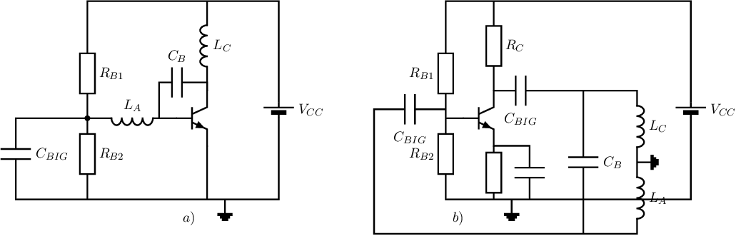
Colpitts in CBC The SSEC of a common-base version of the Colpitts oscillator is shown below in subfigure a), whereas a bare CBC with NPN is shown in subfigure b). Combining these two leads to a first setup for an actual CBC Colpitts oscillator, for which only proper biasing should be checked and ensured (e.g. by adding coupling capacitors or removing excess components). It appears that a direct combination of the SSEC and a bare CBC, leading to the configuration in subfigure c) that satisfies both the SSEC and biasing requirements: it implements a CBC Colpitts oscillator. Note that the (bias) current source that delivers may be replaced by a crappy current source, a.k.a. a resistor.
Colpitts in CCC The SSEC of a common-collector version of the Colpitts oscillator is shown below in subfigure a), whereas a bare CCC with NPN is shown in subfigure b). Combining these two leads to a first setup for an CCC Colpitts oscillator. A direct combination of the SSEC and the CCC, leads to the configuration in subfigure c). This straight forward combination satisfies both the SSEC and biasing requirements: it implements a proper CCC Colpitts oscillator.
In the same way as done for the (many variants of the) Colpitts oscillator described before, Hartley and Clapp (and other) oscillators can be constructed. These other types of oscillators have pros and cons with respect to the Colpitts oscillator. One of the most important pros for students that build oscillators apparently being that the Colpitts is worked out in more detail than the other types of oscillators (for illustration purposes). Anyway, the procedure of constructing a proper single-transistor oscillator circuit is merging the SSEC of the oscillator and the target amplifier configuration (in PNP, NPN, PMOS, NMOS, ...) and making sure that bias conditions are not violated by merging the two (possibly requiring coupling capacitors).
Skipping the synthesis or merging, some examples of proper Hartley and Clapp oscillators are shown below. It way be clear that this is just a very small fraction of all possible implementations! Note also that none of these circuits implements a decent amplitude control: they just implement a very crude amplitude control by clipping. Also note the connections of the inductors (that may mess up bias points due to their DC-wise impedance.
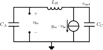
The previous sections in this chapter presented general derivations for harmonic oscillators assuming a single transistor amplifier stage. Those derivations started assuming single-transistor CEC or CSC configuration for which the SSEC is shown in Figure 10.8a. After that extensions towards CBC, CCC, CGC and CDC configurations were made. It was shown that the main difference between all of them, on SSEC-level, is that the virtual ground is moved to another node.
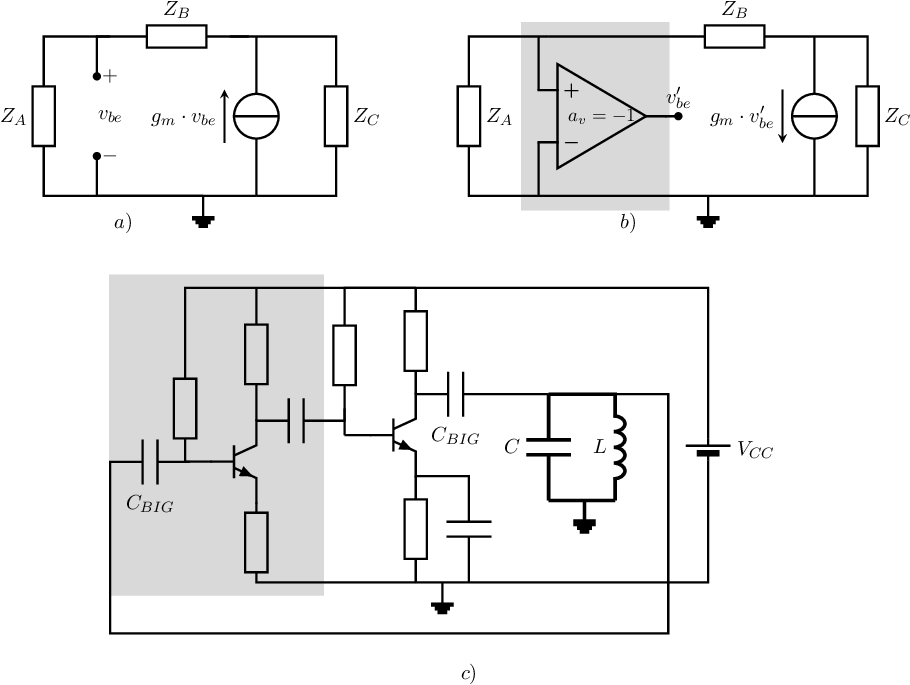
A different type of high Q harmonic follows if the direction (or sign) of the transconductance in the SSEC in Figure 10.8a is changed. The resulting SSEC is simply the one in Figure 10.8b. This flipping of the current direction (or sign) of cannot be achieved with another type of transistor. It can be achieved using e.g. an extra inverting amplifier, a symmetric circuit construction or a transformer. Later in this section, examples are shown.
A derivation of the oscillation condition is almost identical to the one leading to (10.2), the only difference being the sign of the “”. The oscillation condition for the configuration in Figure 10.8b is
|
| (10.4) |
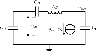
Noting that all impedances are in the first or fourth quadrant of the impedance plane, the left hand side of this equation also ends up in the right hand side of the impedance plane. Noting that is a real positive (trans)conductance, the oscillation condition can be satisfied if and are reactive and not the same type of reactive component. This means that if is a capacitor, must be an inductor, and vice versa. There are no demands on except that it must be conducting, as there must be a feedback loop.
This type of oscillator hence can oscillate properly for:
| C | L or C or R or short | L |
| L | L or C or R or short | C |
Because the simplest implementation for this of oscillators consists of one L and one C and the amplifier, they are usually denoted as LC-oscillators. The amplifier serves to compensate any energy loss during oscillation and effectively implements a negative impedance.
As stated, the big difference between the Colpitts, Hartley, Clapp and Pierce oscillators as compared to the LC oscillators in section 10.5 is the direction (or sign) of the . No single BJT (NPN or PNP), no single MOS transistor (NMOS or PMOS) nor a vacuum tube can achieve this polarity flip. There are however multiple ways to implement this, and some implementations have quite nice properties (that are not relevant in the context of this book).
Prepending an amplifier with negative gain to the effectively implements a negative . Using this leads to the way to implement an LC-oscillator shown below. Note that there are many more similar implementations: the figure only synthesizes one circuit schematic.
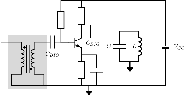
Similar to the previous option where an inverting voltage amplifier was prepended to the transistor, a transformer can be used to introduce a negative voltage gain. This leads to (for example) the following circuit schematic:
Using a negative impedance converter (NIC) configuration implements the voltage controlled current source in Figure 10.8b if . Assuming this , the two-port voltage controlled current source degenerates to a one-port that creates a negative resistance . One way to physically implement a circuit that mimics a negative resistance, and making an LC-oscillator with it, is shown below.
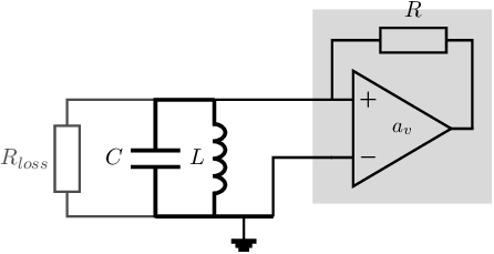
The opamp with the resistor in (positive) feedback configuration creates (at the non-inverting opamp node) an impedance . To get stable harmonic oscillation, and hence to achieve , .
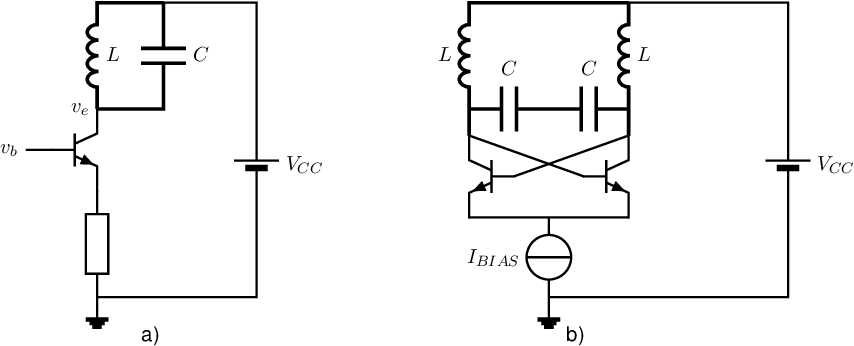
The most widely used way to implement an LC-oscillator is to leverage symmetry in a differential circuit configuration. This symmetry allows to (virtually) invert voltage excursions as required to achieve the (SSEC) configuration in Figure 10.8b.
For that, we start at the schematic shown below, in subfigure a). This can implement a proper LC-oscillator only if with . This was worked out with an explicit amplifier and with a transformer earlier. Now, having this circuit twice, and
can be shown to effectively implement this for both halves of the total circuit. Forcing anti-phase operation can be done — similar to the operation in a differential pair — by keeping the sum current constant and allowing signal excursions in the two halves. This leads to e.g. the circuit schematic in subfigure b).
Quartz crystals — using a component that is constructed from crystalline SiO — are very well suited for creating very frequency-stable oscillators. Quartz is (weakly) piezo-electric, meaning that there is some interaction between the electrical and mechanical domain. The mechanical characteristics as expansion coefficient and modulus of elasticity are not very sensitive to temperature, while there is very little internal friction in crystals. When the crystal is provided with a suitable electric AC voltage, it vibrates mechanically which is then coupled to the electrical domain. The resulting electric behavior is very stable, due to the stable mechanical parameters.
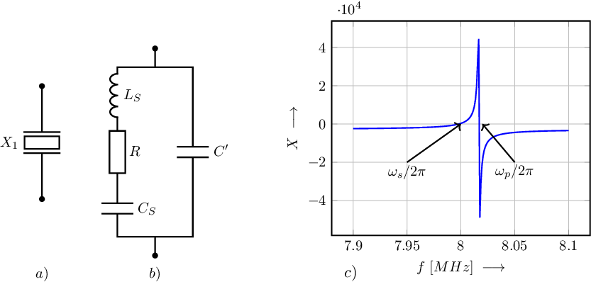
A crystal behaves, from an electrical point of view, like a one port system with an equivalent circuit as depicted in Figure 10.9b. The corresponding reactance as a function of frequency, for a crystal having a resonance frequency a little over 8 MHz is shown in Figure 10.9c. One of the best properties of a crystal is the very high quality factor: Q-factors over are quite common.
The crystal has two modes of oscillation:
series resonance occurs for a voltage controlled (and thus virtually short circuited) case. Then has no influence and the resonance frequency is:
parallel resonance occurs for the current controlled situation (hence with a virtual open connection). The total loop contains and in series, and the resonance frequency is:
The parallel resonance frequency is slightly higher than the series resonance frequency, since .
The numerical values of the parameters and of a quartz crystal with high are somewhat unusual. For example, in the model of a crystal with a (series resonance) frequency of 10 MHz, the parameter as an equivalent to the mechanical mass, is 12 mH, which is relatively large. At the same time, , the equivalent of the (inverse of the) mechanical stiffness is a very small 33 fF ( F). is and represents the internal (viscous) friction. The value of , the electrostatic capacitance between the electrodes, is about 7 pF. This gives a quality factor of 145.000 for the mesh containing , and .
The series resonance frequency and parallel resonance frequency, and respectively, are usually very close to each other, due to the (generally) very small value of compared to the value of . In this very narrow frequency range, the crystal can assume any value of inductance as also illustrated in Figure 10.9c. This means that in any LC-oscillator the L can be replaced by a crystal, and that then the circuit will oscillate somewhere in the very narrow (radian) frequency range between and .
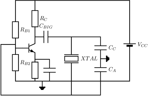
Consequently, the crystal can very well be implemented in a Clapp circuit, due to the resonance characteristic of and , by replacing the series and by the crystal. The now obtained circuit is denoted as a Pierce oscillator.
The inductor of a Colpitts oscillator can be replaced by a crystal, leading to the circuit in Figure 10.10. The crystal is inductive in just a very small frequency band, and in this very narrow frequency band the inductor value can assume any inductive value. Therefore somewhere in this very narrow frequency band the oscillation condition (concerning having a real ) will be satisfied68 .