Radio frequency circuitry (RF-circuits) are different from normal (low-frequency) circuits. One hint in this direction could be the radio within the term itself. With this term, we do not only aim at an AM-radio, FM-radio or such, but at an arbitrary circuit or system that can transmit or receive RF signals. All electronic circuits which have some form of wireless communication are RF-circuits. It does not matter whether it is AM, FM, PM, Bluetooth, IEEE 802.11, GSM, 4G or something else: these are merely the protocols.
Transmitting and receiving data is something completely different from what we have covered so far. The laws of Ohm and Kirchhoff could (almost) always be applied within this book. However, these laws do not allow us to transmit data wirelessly: there is no wire between transmitter69 and receiver, meaning that there is no current loop or voltage mesh. Hence, it would be impossible to transmit information. Compare it with cutting the cord of your iPod earplugs: the current loop is broken, hence there is no more sound70 .
There are exceptions, for example a transformer or a capacitor. A transformer consists of two coupled inductors. One of these inductors is driven by an (AC) input signal and generates a (AC) magnetic field, while the other inductor transforms this field back into an (AC) output signal. The overall result is a fixed ratio between the current and voltage at the primary and secondary side of the transformer, without any wire between the primary and secondary side... A capacitor does not have a true electrical path between the two plates either: there is an insulating layer between the plates. In a capacitor the conduction takes place via charge storage at the plates, as a response to an electric field between the plates of the capacitor. The (AC) current through the capacitor occurs only if an AC voltage is applied.
Both effects in the transformer and in the capacitor are a lot like transmitting — transfer of electric signals without a closed conductive path — and are obviously related to actual transmitting. However, the subtle difference is that in a capacitor and in a transformer the transmitter and receiver are very closely spaced: it’s the other plate in a capacitor or the coupled inductor in a transformer. With a radio system, you are transmitting power, whether or not it is absorbed by any receiver at any distance. More on this later.
The main difference between low-frequency electronics and radio-frequency (RF) electronics is that at low frequencies the voltage law, current law and such are true while at RF the propagation speed of the signals and the theory of relativity are important71 . This is comparable with the fact that Newtonian (mechanical) laws apply for objects at low speeds, but do not apply at very high speeds: relativity starts to come into play. You wouldn’t really notice the effects of relativity in mechanics, but you will in electronics.
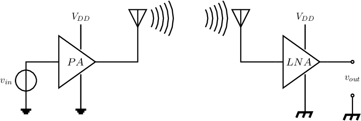
Figure 11.1 shows a basic transmitting/receiving system. At the transmitting side, the signal is amplified with a power amplifier (PA) and fed into an antenna. For simplicity reasons, let’s assume any of the widely applied antenna’s that measure using a regular multimeter.
According to Kirchhoff’s voltage law, current law and Ohm’s law this should yield a zero current in the antenna as there is no closed loop at the output of the PA including the antenna. As a result the (real) power going into the antenna should be — from a low frequency point-of-view — zero. Consequently, zero (real) power would be dissipated in the antenna and hence no power would be transmitted. After reading this chapter, you’ll know better: the antenna generates an (AC) electromagnetic wave from its (AC) input voltage and thereby converts electrical energy into electromagnetic energy. In the electrical domain the antenna then presents a finite and on-zero resistance and may also include a reactive component: the antenna is a device that may store electrical energy but also converts electrical energy into energy in another domain.
A proper transmitting antenna — that can transmit on a specific frequency and/or in a specific direction — can also receive at the same frequency from the same direction. At the receiver side, the receiving antenna72 transforms the electromagnetic wave back to a voltage or current, from which the original can be obtained. Typically a (low noise) amplifier — represented by the LNA block — is present at the receive side to significantly amplify the (small) antenna signal.
The received power by the receive antenna is related to the transmitted power, as described by the Friis equation:
The factors and are the gain factors of the antenna in the direction of the other antenna. Antenna gain and antenna directivity are not covered in detail in this book: only §11.8 touches a number of antenna characteristics, including gain and directivity. For now, let’s simply assume that the antenna is not direction sensitive; then . Hence, within this book, we use:
The relation above already shows that for large distances between transmitter and receiver — which is usually the case — the received power is quite a bit smaller than the transmitted power. In this chapter the focus is mainly on getting a high transmitting power. Since the transmitting and receiving antennae are assumed to be identical, this should also give us a high(er) receiving power. For a high transmitting power, we need:
An RF-system usually transmits a (modulated) sine wave. As you will see further on in this chapter, the antenna can — from an electronics point-of-view — be modelled as an impedance . In this, the real part models the conversion of electrical energy into (here) radiated electromagnetic radiation. The imaginary part models the energy storage around the antenna which is very much the same as energy storage in capacitors and inductors. In conventional circuit theory, energy storage in an element gives rise to reactive power. From this it follows that:
Using conventional network theory, it can be derived that the transmitted power and reactive power are given by:
Where and represent the voltage and current amplitudes; the factor 2 is introduced because of the ratio between effective value and magnitude for a sinusoidal signal. It’s usually easier not to work with the relations above, but with
where can usually be found from an expression including the voltage applied to the feed point of the antennae and the total antenna-impedance. Using Ohm’s law this yields:
This allows for easy calculation of the (real) transmitted power, once the effective voltage (or amplitude or ...) on the feed point of the antenna is known. For example, for an voltage amplitude applied to the antenna:
Little to no attention is paid to modulation techniques. Whether we use an AM-signal73 , FM74 , PM or a digital equivalent ASK, FSK, PSK — possibly multiplexed in time or frequency — or some other modulation technique..
The laws of Maxwell relate the electric field to charge, current and the magnetic field:
Here, is the electric field, the magnetic field and and are the well known operators for vector calculus: the rotation and divergence. As the names of these operations already suggest, these operators calculate how much a vector field rotates or changes. We will not go into these operations and equations: we will work towards a — within the context of this book — usable result. The magnetic field is related to currents and voltages through relativity, meaning that the constants and are related to the speed of light :
It follows from (11.2) that a change in -field causes a change in -field, and vice versa. From the vector operations, it also follows that the -field caused by a time-varying -field is perpendicular to that -field. The same holds for an -field caused by a time-varying -field: this is also perpendicular to . It now can be derived that the power density of the and fields (called an EM-field) is given by the so-called Poynting vector, which is perpendicular to the and fields75:
|
| (11.3) |
The Maxwell equations are an expansion of the voltage and current laws of Kirchhoff. This can also be seen from the equations themselves: for any mesh using the voltage law:
For the same mesh, a similar equation can be written down in terms of electric field strength . The summation then becomes a contour integral — an integral over a closed contour — and results in:
The integral form of is given by . Here, is the total magnetic flux through the surface that is enclosed by the contour. Trying to equate the Maxwell relation equal to the Kirchhoff voltage law relation reveals that:
We can derive something similar for Kirchhoff’s current law. If we take the divergence of Ampère’s law — the Maxwell equation for — then we get76for any 3-dimensional vector:
This relation states that the change in current (density) in a certain volume is due to the accumulation of charge within that volume. This accumulation happens for every current or voltage change, since charge cannot leave infinitely fast from that volume.Trying to equate the KCL to the Maxwell result above, it follows that:
In all previous chapters in this book, the analyses were based on Kirchhoff’s voltage and current law. This implicitly means that the signal frequencies must be low enough: low enough for the wavelength of an EM-wave to be much larger than the physical dimensions of the circuit. For an audio amplifier, which has to operate up to 20 kHz, these assumptions are true if the amplifier is much smaller than 15 km, which is usually satisfied. For a GSM in the 1.8 GHz band however, this already becomes a problem. In this case, the entire circuit must be much smaller than 15 cm to be able to use the current and voltage laws. The internal IC’s within the GSM typically are much smaller than this 15cm and then can be designed and analyzed using the KVL and KCL, but as soon as you connect these ICs with something at the outside — a package, matching network or antenna — then the distances increase to such an extent that the laws of Kirchhoff are not applicable anymore.
A basic rule? Well alright: in general, you may use the Kirchhoff laws if the dimensions of the circuit are smaller than .
An antenna is driven at its feed point by a voltage and transmits an electromagnetic (EM) wave; this course does not analyze the physics behind antennae in detail. From a circuit or system perspective it is only important that the antenna does transmit or receive, and that you can model the antenna behavior by an impedance .
Just as for any impedance, the real part of the impedance transforms the electrical energy into energy in some other domain. In an ordinary resistor the power lost in the resistive component is transferred into heat; in an antenna it is transmitted. The following paper gives a nice introduction into the physics behind antennas; the paper is included with permission from Aspencore / EDNmag.
A dipole antenna is the most basic antenna; the construction of such a general dipole antenna is shown in Figure 11.2. The exact mathematical analysis is out of the scope of this book: only the basics of radio frequency circuits are dealt with therefore knowing basic electrical properties of simple antennas is sufficient. This section therefore only presents some formulas to be able to calculate some electrical properties.
Calculating this can be done using the following set of equations [10], in case you’d be interested or if you want to get a numerical value. The impedance of the antenna connector is related to the “internal impedances” as follows:
The constants and are the wire thickness respectively the free space impedance for an EM-wave In vacuum or air, the radiation resistance of a half-wave dipole antenna equals . If the antenna shows no other significant resistive losses due to e.g. Ohmic losses in the antenna, then the radiation resistance is equal to the resistance of the antenna as a whole.
The impedance of an antenna consists of a resistance and a reactance (inductive or capacitive). For a half wave dipole, the antenna thickness does not seem to be of importance and its reactance in vacuum or air is . For other antenna lengths the relation is dependent on the thickness of the antenna. For the half wave dipole the reactance is — as you can see from the equation — positive for certain values of , and negative for other values. It might seem scary, a negative reactance, but it isn’t. As you know, the impedances of reactive elements are
thus a positive corresponds to an inductance and a negative to a capacitance.
The impedance of a dipole antenna as seen from a driving circuit is shown in Figure 11.3. This figure shows the impedance on the antenna feedpoint as a function of the ratio between antenna length and the wavelength , separating the real and reactive part of the antenna impedance. The figure shows that the antenna impedance can vary between low and high resistance, with a capacitive or inductive series reactance, as a function of the ratio .
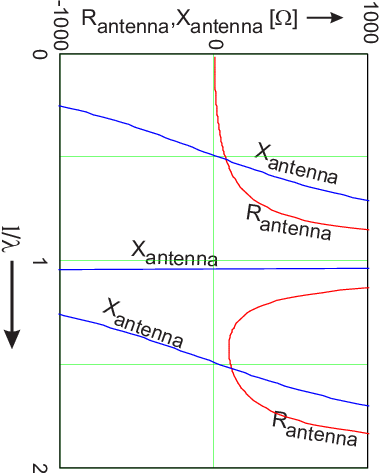
The EM-propagation speed in the antenna is about equal to the speed of light in vacuum from which it follows that for a signal frequency , . Consequently, the x-axis variable in Figure 11.3 is proportional to the signal frequency.
In circuit simulations of transmit (or receive) systems, the impedance of antennas should be taken into account properly. Figure 11.3 shows that the dipole behaves as a system with multiple resonances, at integer multiples of . For quick and not-too-dirty simulations, it may be sufficient to model the antenna at only a few frequencies of interest, modelling the DC-behavior (open for a dipole) and modelling at the transmit frequency (a series construction of a resistor and a reactance, see Figure 11.3).
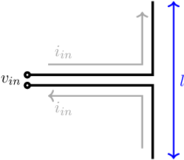
A monopole is just half of a dipole antenna plus a ground plane. A dipole antenna is symmetrical: it is driven at the center and both halves do exactly the same thing concerning the radiation, impedance and some other stuff. This implies that we can identify a symmetry plane in a dipole. Having a symmetry plane in a symmetrically driven structure results in having no net signal at that symmetry plane. This allows us to put a grounded plane at that symmetry plane. If this symmetry plane is sufficiently large, then half of the dipole — the upper half or the lower half — can be removed without the remaining part noticing that (electrically)77 . T Hence, the differences between a dipole and a monopole are small:
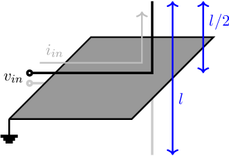
The equivalent of, for instance, a half wave dipole, is now a quarter wave monopole, with:
We can keep on talking about antennas just about forever, but for this introductory course on electronics, that would not be very useful. However, it is useful to get acquainted with a few concepts concerning the antenna: the most important ones are discussed below.
Directivity and gain The terms directivity and gain of an antenna are often mixed up. The directivity of an antenna gives a measure of how well the antenna is capable of bundling its radiation to a specific direction. It doesn’t matter whether or not it is the transmit or receive antenna, since .
a dipole and monopole antenna are symmetric in a (2-dimensional) plane perpendicular to the arm(s). This implies that there is no reason whatsoever that in that plane the radiation in a specific direction is different from that in another direction. As a result, monopole and dipole antennas transmit and receive omnidirectionally perpendicular to the antenna arms.
Note that the receive and transmit power in the direction of the arms is low to zero, due to the same symmetry. sufficiently far away from the antenna then the radiated or received field adds destructively.
Numerically, the directivity or gain of an antenna give the ratio of transmitting power in one specific direction, related to the transmitting power of the isotropic antenna:
where the value of is usually given in : the gain or directivity compared to an isotropic antenna. The gain or directivity of a dipole antenna is . Antennae with a high directivity (or gain) radiate and receive mainly a narrow beam. Antennas that receive signals from many directions (almost) equally well have, by definition, a low gain and low directivity.
Figure 11.1 shows a rather simple representation of a transmit and receive system. The figure below depicts a more complete representation, where the signal to be transmitted is applied to a block that takes care of the modulation onto an RF carrier frequency. For transmitting e.g. audio in the FM band this block changes the oscillation frequency — about a center frequency — in proportion to the input signal. For audio broadcast FM this center frequency is between 88 MHz and 108 MHz while the frequency modulation is lower than 100 kHz. Note that this is a small frequency modulation on a bias frequency: very similar to the biasing and small signal operation of amplifiers.
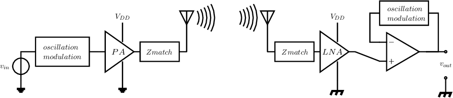
As described in§11.6, the antenna impedance can be heavily reactive (inductive or capacitive) which makes a rubbish load impedance. The (optional) “Zmatch” block between the power amplifier and the antenna ensures that the load impedance seen from the PA is optimal for the PA. This optimum impedance ideally is purely resistive with a suitable resistive value.
The receiver block looks quite a bit like the transmit part. Firstly, the antenna signal is amplified using something called a Low-Noise Amplifier to amplify the small antenna signal without adding a lot of noise. Demodulation can be done in a number of ways. In the figure, the inverse of the modulation operation is used to retrieve the original signal . Also this can be done in a number of ways; the simplest of which is using a feedback system with transfer as shown in Figure 11.5. The only difference with the systems from chapters 6 and 7 is that the opamp block for FM demodulation has its input signal in the frequency domain, with the output signal in the voltage domain. Then the “opamp” input circuit compares frequencies; using the transmitter’s modulator in the feedback loop effectively demodulates the FM-modulated input signal. The hard part is usually getting sufficient gain and sufficiently low noise at the high frequencies used. Diving into receivers is not a subject of this book.
If the physical size of a circuit is much smaller then the wavelength of signals in that circuit, the wave-like nature and the finite speed of an EM-wave does not really have to be taken into account. In that case Kirchhoff’s voltage and current laws can be applied. For example, for an audio amplifier operating up to (let’s say) 20 kHz, assuming that the speed of an EM-wave in a metal is about 2/3 of its speed in vacuum, the wavelength of an EM-wave is about 10 km. Any audio amplifier that is orders of magnitude smaller than that can very well be described and analyzed using the (quasi static) Kirchhoff voltage and current law.
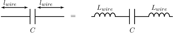
At very low frequencies a wire simply behaves like a short or a low-ohmic resistor. At radio frequencies (RF) this is not the case any more, due to the sheer length of a wire and the finite speed of an EM-wave passing through the wire. There are many models that describe the series inductance associated with wires at RF; one of the more simple ones being the following which is valid for a round wire that is far away from any return ground path [11, 12]:
|
| (11.4) |
where is the wire length in cm, and is the wire diameter in cm.
This translates into — as a rule of thumb — 1 nH/mm wire length. Usually this amount of self inductance is
not that relevant at low frequencies and/or for very short wires, but it may be very harmful already at circuits
operating at 100 MHz with wires that are longer than a few mm. Wires with other shapes or
wires that are relatively close to other conductors exhibit a different relation with wire length.
As example for the impact of a wire, let’s consider a capacitor including wires.
The total impedance of the capacitor including wires is then:
Which can be used to derive an equation for the equivalent capacitance for the original capacitor including wires. This equation is very much (angular) frequency dependent:
Aiming at (arbitrarily) an impedance of , to be used in an oscillator, ideally the capacitance value is
Note that the impact of wires, for a capacitor, is very dependent on both the capacitive value and on the frequency. For example, for a 1 nF capacitor with 2x1.5 mm wires at 100 MHz while somewhat longer wires result in inductive behavior at that frequency.
Example As example of the impact of wire length on circuit performance, a quite straight forward common emitter circuit is used. Assuming 5 mm long wires for /textitevery connection, the following circuit is obtained.
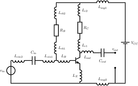
After some simplifications — merging inductances in series — this simplifies to the following circuit. Note that for biasing, the presence of the (inductances associated with the) wires does not change anything. However, for sufficiently high signal frequencies the small signl properties of the circuit may be changed quite a lot. Analyzing/deriving the small signal properties this full circuit is a lot more work that analyzing the original circuit because of the increase component count and it leads to hard-to-read relations.
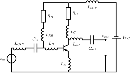
Analyzing the impact of each wire-inductance individually is however straight forward, and the resulting relations are readable and interpretable The impact of the inductances that are in series with the capacitors, and is clearly an impedance in series with the input node and output node.. Assuming that is the only (significant) wire, and assuming that the impedance of the capacitors is small at signal frequencies, the (magnitude of the) voltage gain is lowered and the input impedance is increased.
Similarly, assuming that only has significant inductance, again the input impedance is increased and the (magnitude of the) voltage gain is reduced:
The impact of on small signal properties is mainly an increase in the amplifier’s input impedance. mainly causes an increase of the (magnitude of the unloaded) voltage gain and an increase of the output impedance of the amplifier:
Also note that whereas capacitive effects in transistors — such as junction capacitances in BJTs, see e.g. $2.3.2, §2.3.3 and gate-source and gate-drain capacitances in MOS transistors, see e.g. §2.5.6 are usually ignored, this may not be allowed towards higher frequencies. Typically, at RF these capacitances must be taken into account, which makes circuit design or circuit optimization quite a bit more more complex.
Similar to the single wire case described above, two parallel wires also have self inductance. Because these two wires “see” each other the relation between self inductance and geometric parameters is a little different [11, 12, 13]. Denoting the distance between the wires as and again denoting the wire thickness as , for
Being two parallel conductors, there is also a capacitance between these two wires. Again assuming for , the relation between capacitance and geometric parameters is
From this, two parallel wires can be modelled using (many physically short) sections that have series inductance and parallel capacitance.
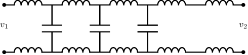
Looking into the pair of wires, this gives rise to an impedance
This means that a signal passing these two parallel wires experience an impedance
while there is
no (NO!) dissipation as there are only inductances and capacitances involved. The impedance only means that there is a ratio between
voltage and current when the signal passes through the two parallel wires; this impedance is typically denoted as the characteristic
impedance of
the pair of wires. Two-parallel-wire configurations are denoted as transmission lines as signals are transmitted through these.
One well known variant of two-wires transmission lines is the “wire over plane” construction. Using symmetry, is can readily be derived (just slide a ground plane in the symmetry plane between the two wires) that then the capacitance (per unit length) is doubled and that inductance (per unit length) is halved,, still using the (now imaginary) distance between the original 2 wires. Denoting the distance between the wire and the plane as this leads to
Another well known variant is the coaxial cable.
If the wavelength of EM-signals is not much bigger than the physical size of components, wires, ..., then reflections occur at any impedance step experienced by a signal. For electrical signals this might at first seem quite strange, but it is simply the same behavior underlying reflections, transmission and more in visible light that happens at a discontinuity in refractive index - you see and experience it every day. This refractive index is nothing more or less than an impedance change for the part of the EM-spectrum that we call light.
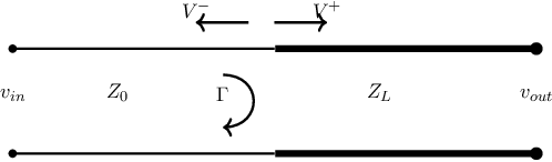
Without digging into details, part of an incident (voltage) wave on an impedance discontinuity is reflected. The reflected fraction is denoted by the (complex) reflection coefficient that depends on the source impedance and the load impedance as
The part of the (voltage) wave that is transmitted across the impedance discontinuity can similarly be described by a transmission coefficient as described below. This has similarities with the theorem on maximum power transfer but it is fundamentally different as this and deal with the reflected wave behavior of EM-waves.
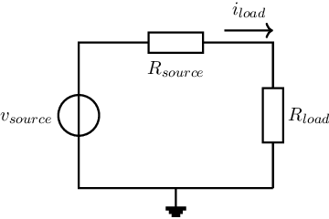
A recap of maximum power transfer and the associated conjungate impedance matching was presented in section 0.21. This assumes an equation for power ending up in a load impedance , for a source with source impedance and a voltage amplitude for the configuration in Figure 11.9.
The maximum power as a function of can be obtained via differentiation:
This directly shows that the power in the load is at its maximum if the load resistance is equal to the source resistance: . In a similar fashion, we find that the power transfer with complex impedances is highest for . A fairly simple result that you can use to design a load. At the same time, you should not use this when designing a power amplifier, or when having voltage or current limitations in the driving power source.
The optimum above holds for the case when you assume an ideal source with a certain — fixed — source impedance, which does not apply if you design your own power amplifier. If you design an amplifier, then you have to deal with limitations in output voltage and output current, and you have a degree of freedom in the output impedance of your amplifier. If you want a maximum output power, then you have to take these conditions into account.
Assuming an ideal voltage source, without any voltage limitation and without current limitation, the power into the load not only depends on but also depends on and . Two additional ways to maximize the power into follows from the following two (partial) derivatives:
that show that
In case you design an amplifier, the output impedance is designed by you, the circuit designer. The second item is usually limited by things like (clipping to) a given supply voltage. As long as no clipping occurs — in voltage or current — the system is perfectly linear and for maximum power into the load, you can minimize the output impedance of the driver/amplifier, maximize the signal swing and use (conjungate) matched load.
Actual drivers/amplifiers always have limitations in output voltage (amplitude) and in output current (amplitude). This is straight forward implication of using non-linear components such as transistors. The current limitation and voltage limitation are properties of (the design of) your circuit and these limitations are usually fairly independent of the load impedance . With current or voltage limitations, (11.5) does not hold and consequently (11.5) (11.5) nor (11.5) are not valid.
Maximum power into is now obtained:
Note that to achieve maximum :
when designing a driver/amplifier and having a fixed , the output voltage amplitude must be maximum and should be minimum and the maximum output current amplitude must be (at least)
when designing the load , the amplifier should be loaded in such a way that maximum output voltage amplitude and maximum output current amplitude are achieved at the same time. Then [14],
Note that this is quite different from the condition of maximum power transfer following from (11.5) and recapped in section 0.21. This is because the derivations above are for maximum power. And more power is more better.
In actual RF power amplifiers, the load impedance that results in maximum power is more complex. The conventional way to estimate this is to apply a variable load impedance (variable real and variable reactive part) and sweep both while monitoring the real power. This approach is called a load-pull measurement or simulation; a good intro is described in [14]. This also shows that conjungate matching is not applied to get maximum power which should be obvious when assuming ideal (but current limited) voltage sources or ideal (but voltage limited) current sources.
Wave-behavior of the RF-signals only kick in if lengths (of e.g. wires, cables, transmission lines, components) are significant compared to the wavelength of the signals. Then reflections as described in §11.14 become relevant and impedance matching should be done to get maximum power in your load. However, do not impedance match directly at the output of an RF amplifier if you want maximum power.