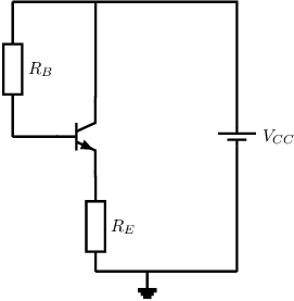
An answer:
Bias = DC ,
,
and assume

This requires some rewriting: separation of variables to get a closed expression for :
An answer:
The voltage drop across
is zero (short at DC), so .
Or you can see it directly from the equivalent circuit for operation at DC in the previous answer.
An answer:
A common emitter circuit (CEC)
An answer:
You can ignore the output impedance of the transistor as long as it is significantly higher than
other impedances at the relevant node (collector). In this case that means that
for signal frequencies.
An answer:
Set DC sources to 0 (in this circuit that is only ).
Assume that the values of reactances for which no values are specified are large. Note that in
this exercise you have to retain
and !
This allows to replace them by shorts or opens: open,
short,
short.
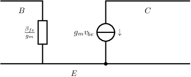
SSEC of the BJT (including B/C/E node identifiers)

Indicate and and redraw. Again: you should (see the description of the circuit) not replace , by shorts!

An answer:
In this answer, the output port is driven from an independent voltage source driving the output
port. The other independent sources need to be set to zero. The corresponding small signal
equivalent circuit is given below. This will be used to derive .

An answer:
Using the SSEC from question e) to calculate the voltage gain
can be done as follows.

This SSEC can be simplified by capturing and into one impedance
A derivation can be done as shown below:
Now back substitution leads to the/an answer: