An answer:
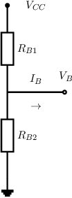
is the voltage at the base node, which generally cannot be calculated merely assuming and form a resistive divider and hence applying the formula for that. This can easily be seen in the circuit schematic depicting the voltages and currents at and around and .

From this can be derived. Formulating KCL/KVL:
leading to
Or applying superposition you get the same equation in a different appearance:
This yields:
This yields numerically
An answer:
When the signals are sufficiently small so that we can approximate the non-linear transistor
characteristics by a linear function.
An answer:

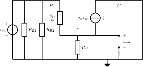
Which can be redrawn (simplified) into

To calculate the output resistance, e.g set and force a voltage at the output . Then calculate the current delivered by and apply Ohm’s law.