In the previous chapter, two components with larger-than-unity power gain were reviewed: the bipolar junction transistor (BJT) and the MOS-transistor. Both types of transistors are strongly non-linear, while the controlled output current only flows in one direction.
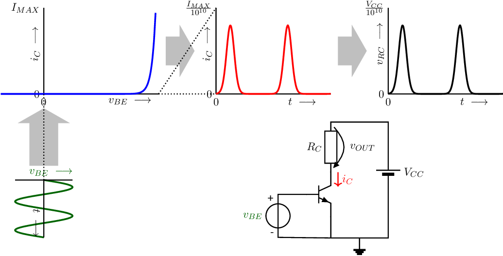
A very basic voltage amplifier is shown in Figure 3.1. In this circuit schematic, the (sinusoidal) input voltage with in this example a magnitude of about is applied to the NPN’s base-emitter port, while the resulting is converted to a voltage drop across resistor . In equation:
Clearly the output current is not a sine: it is heavily distorted and the NPN’s collector current is very low as is the voltage across . This is also illustrated by the signals in Figure 3.1. In the graphs in this Figure, is defined as .
In this figure, the input voltage (as a function of time) is shown in the lower left corner. Note that this graph is rotated, having the x-axis (time axis) pointing downwards. The resulting collector current can easily be constructed by mirroring the input signal in the non-linear -curve shown in the left upper corner. This yields the graph. Note that the y-axis of this graph is heavily zoomed with respect to the y-axis of the graph is order to see the current. The rightmost graph in Figure 3.1 shows the voltage across as a function of time; this voltage is simply . Note that this graph’s y-axis displays just a tiny bit of the supply voltage in order to see any voltage. Note again that and are very small and are far from sinusoidal: they are heavily distorted.
The very small magnitudes of and in Figure 3.1 can be increased by increasing the input signal’s amplitude, but this causes an even more distorted and that do have larger amplitudes. Figure 3.2 shows the situation in Figure 3.1 but with a 2.5 times larger input voltage.
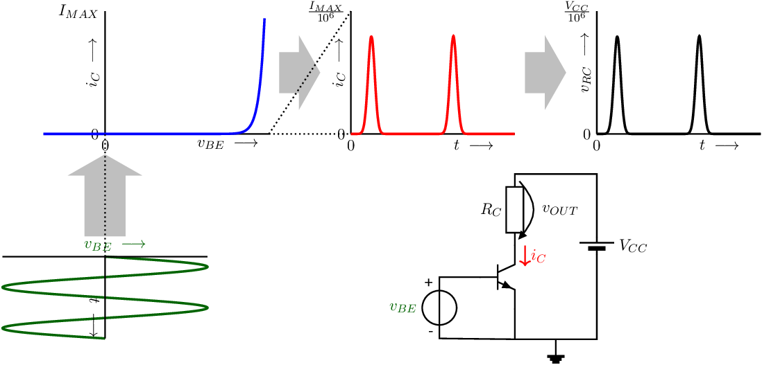
The main problem with this amplifier circuit is that its input signal goes positive and negative — where the transistor is mainly off during the majority of the input voltage — which translates into the rather small and heavily distorted output current. Proper biasing of transistors can solve this, and is the subject of the current chapter.
As a starting point for properly biasing a transistor, again the simple amplifier circuit of Figure 3.1 is assumed. For the principle however, it makes no difference whether we choose a different configuration or whether we would use a MOS transistor, vacuum tubes or something else with electrical power gain larger than 1. The general principle of such circuits is:
For transistors (and alike) there are two other (very much related) properties that yield requirements on proper biasing:
From this, it follows that to amplify an input signal with some degree of linearity,
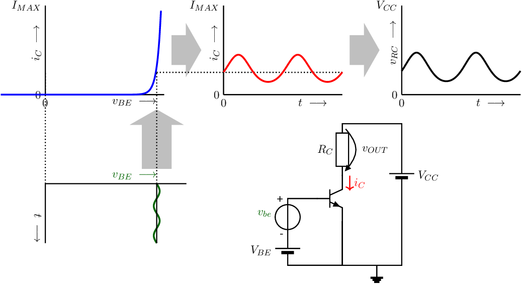
This preprocessing can be achieved by superimposing the input voltage variation (that can go positive and negative) on a larger DC-voltage and ensuring only a small relative current variation. The DC-voltage or its corresponding DC-current is called the bias point, operating point or quiescent point of the transistor. Figure 3.3 shows a Common Emitter Circuit (CEC, see chapter 5) that is biased in such a convenient bias point. In Figure 3.3 the input signal is a factor 10 smaller compared to the situation in Figure 3.1, although the output current is significantly larger and the circuit now works considerably more linear (actually: less non-linear). Note that the graphs in Figure 3.3 do not use scale factors for the current and voltage axes in the rightmost two graphs.
There are a number of requirements for a proper bias point of transistors in circuits. Because the output current of a transistor is a well defined monotonous function of its input voltage, it does not matter whether the bias point is defined in terms of driving voltage or output current. For a proper and stable bias:
The circuit must operate properly for varying temperatures. Variations in temperature are usually due to the environment and the dissipation in the electronic component itself. If the temperature changes, the collector current (for a BJT) or the drain current (for a MOS transistor) changes significantly for a fixed input voltage ( respectively ). A suitable bias circuit decreases this sensitivity to temperature significantly.
When producing electronic components there is always some spread in the components due to tolerances in the production process19 . For example the spread in current gain of a bipolar transistor can amount to 50%; the spread of is also significant. In MOS-transistors, the spread is mainly in the threshold voltage and in the current factor .
The input signal of a transistor appears as a variation around the bias point. Hence, the bias point has to be chosen in such a way that the signal is amplified in a sufficiently linear fashion. Usually, this means that the current variations have to be small compared to the bias current20 .
Due to plain physics, the output current of a transistor cannot change sign and hence, to avoid high distortion levels or even clipping, a transistor must be biased at a bias current that is larger than the maximum desired current variation. Translated to the “input” of the transistor, this is equivalent to biasing the transistor with an input voltage ( or ) that is larger than the signal voltage variations superimposed on it.
The bias current is set by applying a well-defined bias voltage to the transistor. Since a BJT also has a well-defined relation between the base and collector current, a bias current for a BJT can also be set using a bias base current. Concluding, we can bias a transistor by:
For sufficiently linear behavior, the variations on the transistor’s input voltage must be sufficiently small. The other way around: for small input voltage variations, the transistor’s operation is quite linear, and normal linear circuit analysis techniques may be used for evaluation of its (modelled) behavior21 .
In this chapter, we describe the methods for obtaining a well defined bias point. In chapter 4, a linear equivalent circuit for transistors is derived that describes its behaviour about the bias point, and in chapter 5 we give some examples of amplifier circuits, where the small-signal equivalent circuits of chapter 4 are applied.
Before we go into the details on how to bias a BJT, it might be useful to recap the element equations:22
As stated in §3.4, there are many methods for biasing a BJT that essentially boil down to forcing a certain bias current and its corresponding bias voltage .
The easiest method for forcing a collector current is using a DC-voltage source that provides a , as in Figure 3.3. and in Figure 3.4a. For transistors that have to deliver a DC current this is quite sufficient provided that the DC-voltage can be set sufficiently accurate and provided that for the transistor’s operation on signals, the does not have to change. This latter is usually not satisfied.
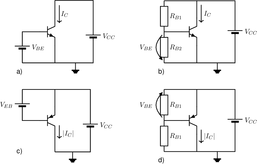
Another disadvantage of this method is that it is rather sensitive to variations in temperature due to the temperature dependence of the BJT. It can be derived that typically 1 K increase in temperature already results in an increase in of about 7%23 . However, an advantage is that the base current drops out of the equation which means that the circuit is insensitive to variations in current gain .
An alternative to the circuit in Figure 3.4a is the implementation (with relatively low ohmic resistors) in Figure 3.4b.
Bipolar transistors can be biased to a certain DC-current in various ways. When the current gain is known, the easiest way is to “force” a DC-base current , which results in a DC-collector current . From a fundamental point of view, forcing a base current has to be done using a current source, as shown in Figure 3.5a.
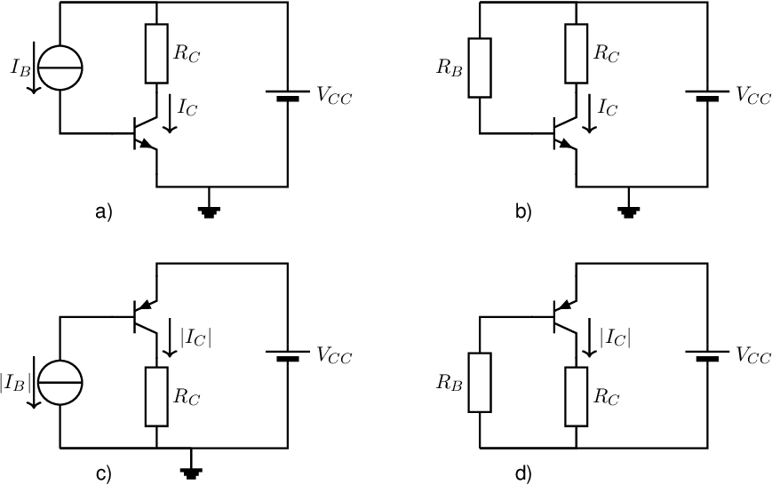
Theoretically, this is a good method to set a bias as long as the current gain factor of the BJT is known and is sufficiently constant. This is reasonably insensitive to variations in temperature, but can vary significantly between BJTs.
Using ideal current sources to bias BJTs is fairly easy, but also purely theoretical. In reality, there is no such thing as an ideal current source: they are always composed of passive (R, L, C, ...) and/or active (MOST, BJT, ...) components. Provided that the output impedance of such a circuit is very high — compared to the impedance of the BJT base-emitter junction’s impedance – the bias circuit may be modelled as an ideal source.
In many circuits, the ideal current source of Figure 3.5a is implemented with a quite simple highly non-ideal current source: a resistor, see 3.5b. The value of is set by selecting an appropriate value for resistor . Using the brute force approach a suitable is easily derived assuming that is known:
For synthesis applications — where you determine the behavior — can easily be expressed in the target that you want to set as bias condition if you know the element equation including its constants. Then you can directly calculate the required value . No problem.
For synthesis applications where you do not know all BJT parameters cannot be expressed in the target ... some parameters are missing. Then there is no way to exactly calculate the required value . Using a smart trick — or a fair assumption — the calculations can be done.
For analysis, where you are given and may be asked to calculate this is a major problem. In that case you would have to solve which is very hard since it involves solving an equation including an exponential relation and at least one linear relation. Although that may seem easy to solve, it actually is quite nasty, near impossible. Using that same smart trick — or a fair assumption — also these calculations can be done.
A good assumption or model (in terms of accuracy and simplicity) is that the of a silicon bipolar transistor at room temperature is typically between 0.6 V and 0.7 V. This stems from some physical properties of silicon and from the fact that due to the exponential relation for every change in by only the current changes by a factor 2. For a change in by the collector current then changes a factor 10. The other way round, for any sensible current the for silicon BJTs ends up between 600mV and 700mV. If you really stress the transistor it may be as high as 800mV. Consequently, a fair estimation for for silicon BJTs is:
| (3.1) |
Although the choice of 0.65 V seems arbitrary, it does give a result with reasonable accuracy:
the voltage varies just a little with collector current, due to the logarithmic dependency (with scale factor ). For e.g.
It can be concluded that if the BJT is biased properly, the errors introduced by the assumption are usually small, while the calculations are simplified enormously. If you do not like the 0.65 V, please use 0.7 V or some other easy-to-use number in that (silicon) ballpark.
Advantages of setting a bias current using a base-series-resistor include:
A disadvantage is the large sensitivity to spread in . For unselected discrete transistors of one production series, the value of can vary up to 50%, which means that for every new transistor, a different resistor value must be set to get the same . In a production facility this would be a huge problem while it is not in a laboratory (as long as you do not change the transistor). A possible solution for this spread sensitivity is introduced in the next section.
The main disadvantage of the bias methods introduced above is that sensitivities to component spread, having inaccurate component values, temperature fluctuations, ... is significant. These disadvantages can be mitigated using some form of “self-correction”, which is applied in just about every real circuit. This self-correction assures that variations are counteracted by the circuit itself. There are many different methods for self-correction24 . The general term for these effects is feedback. In other chapters in this book, feedback is explained in detail. For now, we use relatively simple feedback configurations.
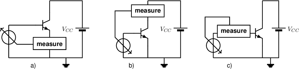
In feedback circuits, the measured quantity is compared to the desired value, then (in this chapter) this measured difference is used to minimize the difference between the two. For a transistor circuit, we could for instance measure the output (collector or drain) current and use this measured quantity to get and keep this current at a specific value. This leads to 2 possibilities to implement feedback:
A third method is to measure the and adjust the to obtain the target ; this method assumes that the is sufficiently accurately known. Figure 3.6 shows these three methods. Note that these methods depict simplified situations for circuits with one transistor where (a measure for) the collector current is used to adjust the transistor’s in order to get a stable and well defined bias current . The principle can be generalized to feedback around an arbitrary system.
An often used feedback method measuring the bias current at the emitter (or source) side is called emitter degeneration (or source degeneration for a MOS transistor). In Figure 3.7, this emitter degeneration is shown for an NPN transistor. The circuit counteracts variations in the bias current ( and/or ) due to e.g. temperature changes, component spread, ageing, and much more.
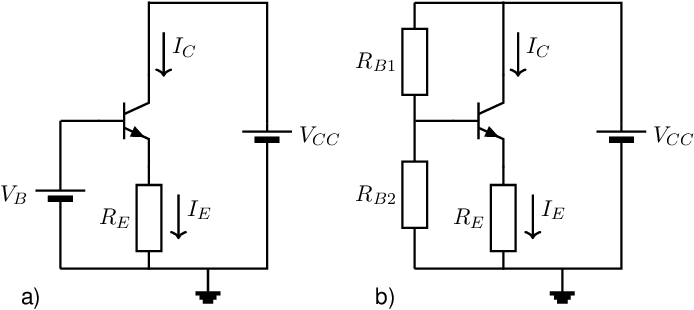
Let’s assume — for illustration purposes — that the temperature of the transistor increases. Due to some the semiconductor physics that determines the behavior of the BJT, for a constant the transistor’s and increase with about 7%/K. With the circuits shown in 3.7, this increasing results in an increase of the voltage drop across . Assuming — for simplicity — a constant base voltage , the increasing emitter voltage results in a decrease of which counteracts the initial increase of the and .
In the circuit of Figure 3.7a, the collector current of the BJT is set by applying a base voltage, and using emitter-degeneration (feedback via the emitter current and emitter voltage). Synthesizing or dimensioning a circuit — forcing the circuit to do what you want it to do — can be done in an exact way:
where is the bias current. for the BJT For this, you have to know the element equations including the constants in it. If e.g. the in the transistor’s element equation is unknown then you have to make assumptions, such as in the derivation.
Note that implicitly this derivation assumes that there is a certain amount of feedback via . If (in the previous equation) is chosen to be equal to the required to get your target then the voltage drop across is zero, yielding and consequently then there is no feedback. It can be derived that to have significant feedback to get a stable operating point for an NPN or PNP
For analysis the resulting bias current now follows from some straightforward math:
This looks quite simple. It is however not a closed form expression as is on both sides of the equation. Solving this analytically can be done using the nasty Lambert-W-function, but that does not give insight or useful results. Using the previously introduced assumption that for a properly operating silicon NPN and assuming that for proper emitter degeneration:
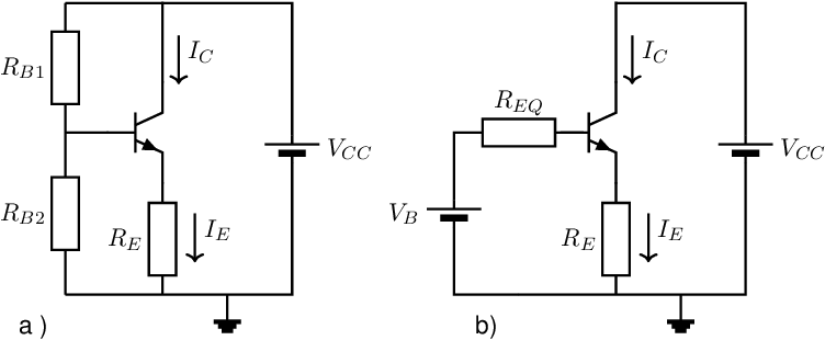
In Figure 3.7b the base voltage is set by resistors and . If this voltage divider has a low impedance, then the base voltage is not (actually, hardly) a function of the base current. In that case , which gives effectively the configuration in Figure 3.7a.
If the voltage divider is not low ohmic, then the base current does have an effect on the base voltage. The bias current of this circuit can be calculated by using brute force, but it can be simplified using divide-and-conquer. In this case, using a Thévenin representation of the resistive divider and the voltage source simplifies things considerably. The resulting equivalent network is shown in Figure 3.8b with and .
Then it can be derived that:
Note that now feedback is implemented via both and that both are related to . Due to the ratio between and the impact of the feedback via is however lower by a factor but typically can be designed to be much more high-ohmic than . Neglecting its sensitivity to variations in , operating point stabilizing feedback via , can also be a useful approach, as alternative or in combination with emitter degeneration. Note that this feedback is the highest for and can be made more efficient than feedback via if variations in and dependencies can be neglected.
Example: suppressing variations in temperature
A BJT is biased at a collector current of 1 mA. For this transistor, the
at constant current changes by -2mV/K. With the exponential relation between
and
,
, this corresponds
to increase
in per
at a constant
. For a temperature rise of 100K
this amounts to an increase in
by a factor .
Q: Calculate the required value of
if the collector current is not allowed to increase more than 10% with a 100 K temperature increase. You may
assume that the base voltage for this transistor is fixed.
A: For the given temperature shift:
Now, both the variation in voltage and the allowed current variation are known. From Ohm’s law,
with
yielding
. Note that this is the
lowest value for ; for
larger values of ,
the change in current is lower.
Note:
For the lowest value of , there already is a voltage drop of 2 V for a bias current of 1 mA. A higher level of insensitivity requires a higher resistance, that requires a higher voltage drop across that resistor.