This chapter presents a brief introduction into semiconductor physics and the behavior of the most important nonlinear electrical components: the diode, the bipolar junction transistor (BJT) and the MOS-transistor. At the end of this chapter you should have a basic understanding of the operation of semiconductor components. The theoretical underlying physics and other in depth stuff is outside the scope of this book.
Non-linear components14 are required in any system that:
requires power gain larger than 1. Power gain is used to boost small signals to a sufficient power level, but is also essential to compensate for signal losses in a system.
In components with power gain (larger than 1) usually a large output power is controlled by a much smaller input power. The difference in output power and input power (and dissipated power!) is supplied by some energy source, which usually is a DC current source or DC voltage source: at . Because the frequency of the DC sources is in general very different from the frequency of the signal to be amplified, frequency conversion is necessary. Since frequency conversion is not possible with only linear components, every amplifier with more-than-unity power gain requires nonlinear components.
The electrical conductance of any material is determined by both its lattice structure and by some properties of the atoms in the lattice. In semiconductor physics typically a nice regular lattice is assumed. Then the electrical properties of the material are completely determined by the atoms, or more specifically by the band structure of the atoms in the lattice.
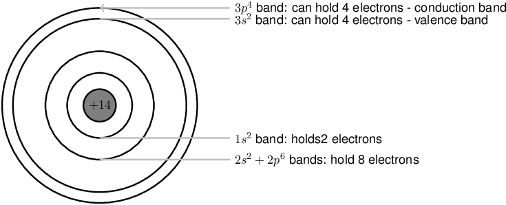
An atom consists of a nucleus, surrounded by bands, each of which can contain a specific number of electrons. Now, the following situations can be distinguished:
From an electrical point of view, most of the bands in an atom are not very interesting:
Therefore, from now on, we only consider the two outermost bands of a (semi)conductor that contain electrons. The outermost of the two is denoted as conduction band, while the inner of the two is called the valence band.
In any semiconductor, the valence band can hold (per atom) as many electrons as there are electrons available for this band: the valence band can hence be filled exactly. If this is the case then there are no electrons left for the conduction band, which thus remains completely empty. The semiconductor now acts as an insulator.
The nice thing about semiconductors is that the valence band and conduction band are close to each other, making it possible for electrons in the valence band to gain enough (thermal or electrical) energy to “jump the gap” to the conduction band. Once these electrons are in the conduction band, they may lose energy and fall back into the valence band15 .
Once an electron has evaporated from the valence band, across the band gap to the conduction band, it has an enormous amount of space to move around freely: such an electron (negative charge) can contribute to the electrical conduction. At the same time, that electron leaves a void behind in the valence band, which is denoted as a hole. The charge of a hole is positive: it corresponds to missing one electron. The hole can also contribute to the electrical conduction. Note that moving a hole through a lattice is due to subsequent moving electrons into that hole: the hole moves therefore in the opposite direction of the electrons!
Because the movement of a hole is due to subsequent movements of different electrons, one might already guess that the electron in the conduction band can move easier than the hole in the valence band. The ease of moving through the lattice for both the electron (negative charge carrier) and the hole (-electron, positive charge carrier) are usually described by its mobility. The mobility tells you how much speed (m/s) you can get in some electrical field (V/m), making the unit of mobility , or more commonly used in the field of semiconductors . In silicon the mobility of holes is about a factor 2 or 3 or lower than that of electrons.
The most commonly used semiconductor is silicon (Si), whose valence and conduction bands each can hold 4 electrons per atom if it is in a mono crystalline solid state. Since it is a ‘group IV’ atom in the periodic table it has 4 electrons available for those 2 bands. The distance between the conduction band and valance band is such that at room temperature a few electrons in the valance band can get enough energy to jump into the conduction band: it is a semiconductor16 .
Semiconductor materials with only one flavor of atoms are boring and not very useful. This is why we use doping to make multiple favours of doped semiconducting material.
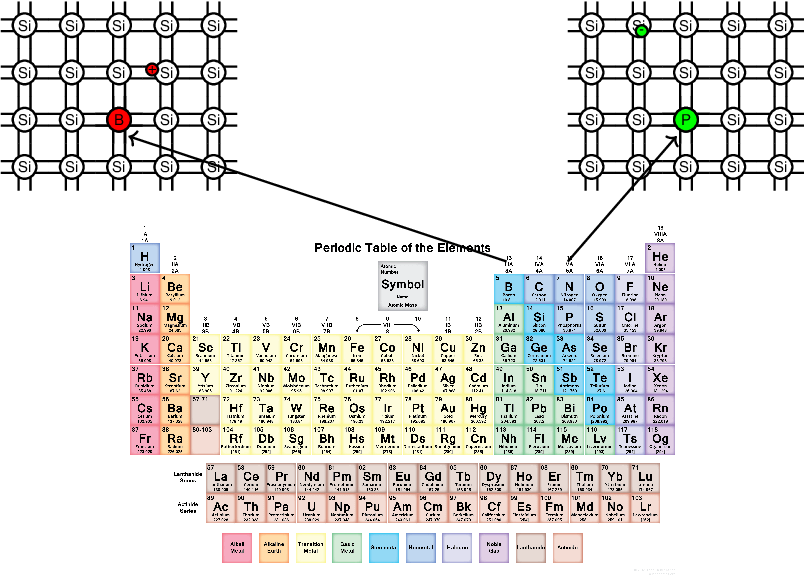
Electrons flow from a lower potential to a higher potential, whereas holes move in the opposite direction, towards lower potential. This seems strange, but it is because at around 1900 A.D. some guy defined this the wrong way and now we have to deal with that forever.
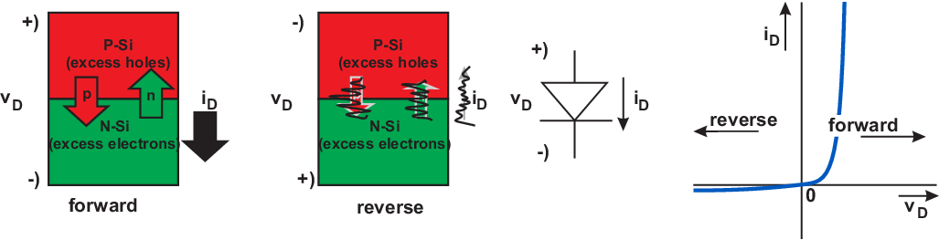
Now, assuming a semiconducting lattice, one half of which is N-doped (excess electrons) and the other half having P-type doping atoms (excess holes), then:
using equations for drift and diffusion, it can be derived that the actual voltage-current relation of the diode is:
where depends on the semiconductor material, dopant levels, size, and is very much temperature dependent. Further, is the elementary charge, the Boltzmann constant and is the absolute temperature. The factor is the voltage applied across the P-N-structure.
Such a component is usually called a pn-junction or diode. In a diode, there can hence be two major current components (and two minor ones that make up the leakage current and that are neglected here): an electron current from n to p and a hole current component from p to n, if the potential at the p-side is higher than that on the n-side. Both of these major current components contribute to a conventional current (in Ampère) in the same direction: from p to n, since electrons and holes are oppositely charged and flow in opposite directions.
It was stated earlier that the diode current-voltage relation in a quite-a-lot simplified case is
One might be tempted to think that the only temperature dependency is due to the term between brackets, that includes the absolute temperature . Due to this term alone, at constant the diode current would decrease with increasing temperature . However, the factor in this relation is actually also heavily temperature dependent and increases with increasing temperature . A (still simplified) relation for including material properties and sizes is:
Especially this is quite temperature dependent. It depends on the so-called density of states, the material bandgap and on thermal energy. In equation this translates into
An expanded version of the voltage-current relation of a diode, including temperature effects, would be
The combination of the various exponential terms in this (expanded version of) in combination with results in a diode current that (at constant ) increases about exponentially with temperature around room temperature. As a rough guideline, the diode current (at constant diode voltage) doubles for every 10K increase in temperature. The other way around, at a constant diode current, the diode voltage decreases about 18mV with a 10K increase in temperature.
As argumented in §2.3, holes from the P-doped part in a junction diffuse towards the N-doped region, and vice versa. Being initially unchanged materials, after diffusion of mobile charge carriers, in both the P-region and the N-region ionized atoms are left behind. These ionized atoms form a so-called depletion layer around the metallurgical junction where (nearly) all atoms are ionized. In this layer, the charge is associated with the ionized atoms and hence are not mobile. The amount of depletion charge is a function of the applied voltage, and can be written as . Because the charge is dependent on the applied voltage, we now can define a (non-linear) depletion capacitance
Using in-depth semiconductor physics derivations, the exact can be calculated. Using the fact the the charge is (almost entirely) stored as ionized atoms, it can be derived that the width of this depleted layer, assuming uniform dopant density in the P-region and in the N-region is
Here is a the so-called built in voltage that depends on the (fixed) material and dopant levels and weakly depends on temperature. Noting that in the depletion layer there are almost no mobile charge carriers, a pn-junction is very similar to a plate capacitance where the plate distance equals the width of this depletion layer . This equivalence is depicted in the figure below:
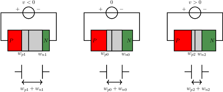
The capacitance for a plate capacitor is given by :
| (2.1) |
where the distance between the plates is and the area of the plates equals . Using this to get the capacitance associated with a the depletion layer in a p-n junction, it follows that (assuming uniform dopant levels in both the N and P region)
For most dopant profiles, it can be shown that this relation can be rewritten into something like the following relation. Note that this presents a capacitance that depends on the material, the dopant level, depends weakly on temperature AND depends on the applied voltage.
Operating a junction in forward, an appreciable forward current occurs already at a relatively low forward voltages. This current is due to diffusing majority carriers: holes from the P-region to the N-region and electrons from the N-region to the P-region. These current components are exponentially dependent on the applied voltage. The diffusing majority charge takes some time to diffuse from one side of the depletion layer to the other side, which can be modelled as an apparent charge storage effect: as a capacitance. Introducing a lifetime parameter that models the time it takes for a charge carrier to diffuse, the total charge associated with forward currents is
| (2.2) |
and consequently the diffusion capacitance is
| (2.3) |
Note that this models a (very much) voltage dependent capacitance for the forward biased junction. This capacitance adds to (and can be dominant over) the depletion layer thickness related capacitance in section 2.3.2.
A sufficiently accurate model of the diode is now the combination of all previous voltage-current and voltage-capacitance relations for p-n junctions:
About all “constants” in these relations depend on dopant levels, physical dimension, the material and the temperature. The diode symbol, with voltage and current convention and the i-v and C-v characteristics for some silicon diodes are shown in the figure below.
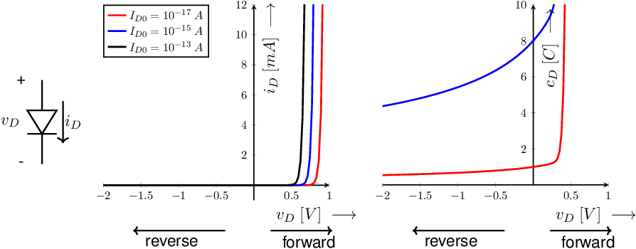
In the graph in the middle of Figure 2.6, current-voltage curves are shown for 3 different values of . These different correspond to (silicon) diodes with very different physical sizes. Note that — due to the exponential nature of the i-v-relation — all i-v curves have the same shape but appear to be shifted on the -axis.
The graph on the right hand side shows the diode capacitance as a function of . Again, the two curves correspond to (silicon) diodes with different sizes and dopant levels. These -curves are relatively flat in reverse, i.e. for and are quite steep in forward.
On a linear-linear plot, the exponential relations appear to (nearly) zero, below some specific while the i-v curve seems to rise rapidly above that . This can be observed in e.g. Figure 2.6. where that is somewhere between 0.6 and 0.8 V. Zooming in on (or out) an exponential curve yields the exact same curve, only shifted left (or right)17 . Therefore, the voltage at which the -curves appear to increase sharply in Figure 2.6 may seem quite arbitrary.
However, the performance of silicon diodes in forward is quite good if the forward voltage is between about 0.6V and 0.7V. The ins and outs of this are outside the scope of this book18 .
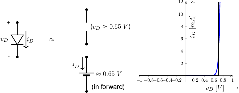
Operating a silicon diode between 0.6 V and 0.7 V results in a diode current range of almost a factor 100; the other way around: can be kept in the range between 0.6-0.7 V for a large range of . Noting that for that large -range the does not change significantly, a silicon diode in forward may be modelled as a DC voltage source having a voltage of about 0.6... 0.7 V.
Having a significant current at results in having a much lower current below . A frequently sufficiently accurate model for a silicon diode is that the diode current is (near) zero for . This behavior can be modelled as an open.
Combining these crude simplifications lead to a model for a (silicon) diode that is sufficiently accurate for many situations: behaving (almost) as an open for lower than about V and behaving (almost) as a voltage source for positive diode currents :
A Bipolar Junction Transistor (BJT) is a smart extension of a diode. In a diode, holes move from p to n and electrons flow from n to p, where for both current components the -relation is exponential:
In a diode, both current components flow through the diode and through the same terminals. They must, since there is no other place to go in a device with only two terminals... However, in a BJT one of these two current components is redirected to a new — third — terminal that collects this redirected current component. Unfortunately, the other current component is still present and this current component represents an unwanted — drive — current.
There are 2 types of BJTs:
The behavior of these two types of bipolar transistors is the exactly the same, except for the type of charge carrier. This difference results in a change of current direction and a change of polarity of the voltage on the terminals. Usually the NPN transistor is easier to understand than the PNP transistor: there are less minus signs involved in its element equations. That’s the main difference, really.
A schematic view of the principle of the operation of BJTs is shown in Figure 2.8. Right next to the cross sections of the NPN and PNP are the schematic symbols for these transistors. The emitter is identified by the arrow; the direction of the arrow is in the direction of the current flow in [A]. The collector is the opposite terminal and the base terminal is in the middle. The symbol itself resembles the physical construction of the very first bipolar transistor as constructed at Bell Labs in the late 1940s.
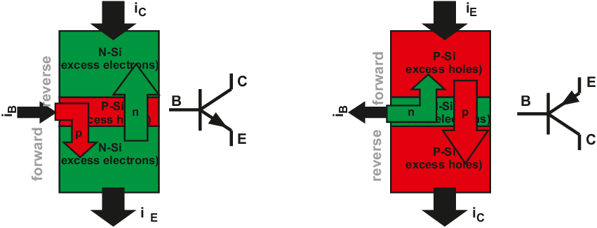
In order to get significant currents, one of the junctions must be in forward. That way, both a large electron and hole current component result. Only one of these components will be directed to the third terminal to create the output current. To ‘catch’ this wanted component the other junction must be in reverse (or at least far less in forward). Naming the parts:
Summarized in equations, the behavior of a BJT resembles that of a diode. If the BC-junction is in reverse — which is the case in the normal operating range — we have for an NPN transistor the following element equations..
For its PNP-equivalent the currents and voltages are inverted, but the equations are (up to minus signs) the
same.
Similar to the situation for the diode, depends on the semiconductor material, dopant levels, sizes, and is very temperature dependent. The assumption that the BC-junction is in reverse is actually not necessary: the actual requirement for proper operation of a BJT is that the BE-junction is much more in forward than the BC-junction. Noting that the current-voltage relation of a junction is exponential it is sufficient to satisfy (for an NPN)
and assuming that a current ratio of 100 satisfies this “much bigger” we get (again for an NPN)
For the PNP-equivalent you should include a ”-”-sign for the voltages. If the is smaller than about 100mV, an explicit -dependency must be included:
| (2.5) |
The operating range in which the second term on the right hand side in (2.5) is significant, is called saturation and hence is for . In saturation, the collector current changes strongly with .
Figure 2.9 shows the collector and base currents of a BJT as a function of and , on linear axes. For the curves, a typical was used, resulting in a hardly visible curve. In the plot 3 curves are shown, for values each 18mV different. Due to the exponential dependency, each 18mV difference in results in a factor 2 difference in at room temperature.
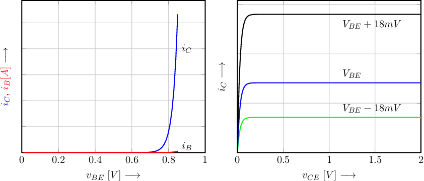
The voltage-current relation of the BJT is quite similar to that of a diode. The impact of temperature is also pretty much the same. Hence, the collector current (at constant ) increases about exponentially with temperature around room temperature, showing a doubling for every 10K increase in temperature. At fixed collector current, the decreases about 18mV for every 10K increase in temperature.
The ideal(ized) element equations for the bipolar junction transistor are listed below. In this section we ignore any dependency in the pre factor for simplicity reasons. Assuming that the BC-junction is sufficiently in reverse, idealized, from (2.4),
Without the explicit assumption of having the BC-junction in reverse, the collector current-voltage relation is, from (2.5),
| (2.7) |
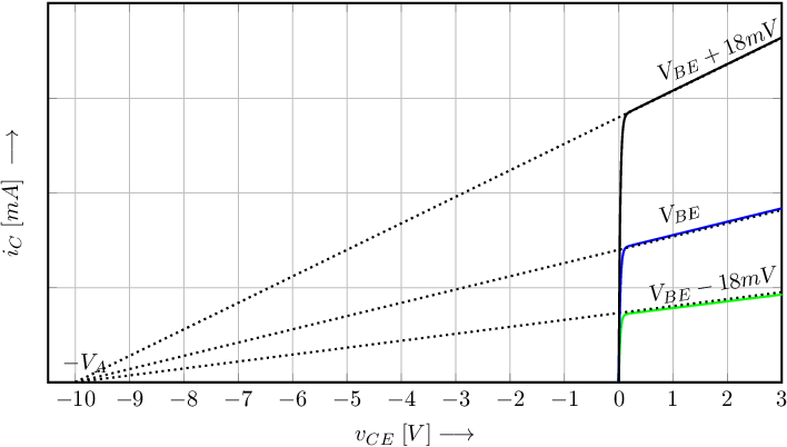
The last term on the right hand side in this relation is significant for roughly . Also in this voltage range the current gain shows a significant voltage dependency. Another voltage dependency of the collector current is that the collector current increases with higher voltages, due to the so-called base width modulation. With base width modulation, the thickness of the depletion layer associated with the BC-junction increases with increasing and thereby modulates the effective (not depleted) width of the base region. The figure below shows the impact of this base width modulation on the collector current . It appears that extrapolated -curves cross the axis in about the same , leading to
| (2.8) |
In this relation is a transistor-dependent constant, usually denoted as the Early voltage, named after one of the early guys modelling this effect.
A bipolar junction transistor consists of two junctions that both have capacitive effects similar to those described for individual junctions. The junction between base and emitter is in forward in normal operation of the transistor, while the collector-base junction typically is in reverse. Their voltage dependent capacitive behavior is very similar to that described in §2.3.2 respectively in §2.3.3.
In literature, there are multiple ways to define the current gain of a BJT and there are even multiple names for each of these ways. The two usual ways to define the current gain are:
where the “f” in the subscript denotes regular forward operation of the BJT. The second letter in the subscript denotes the reference node. Hence, with the “fe” subscript, forward operation is assumed having the emitter as reference node and hence having as “free” terminals the base and the collector nodes. The symbols that are typically used for this are , and . In this book, is used. Typically and consequently , usually for discrete BJTs.
Using the base as reference node, the current gain is and the symbols used then are , and . In this book, this way of describing the current gain of a bipolar transistor is NOT used. Note that and hence with a large , the is a little smaller than 1.
MOS transistors in a nutshell. MOS transistors are barely used in the Advanced Technology track, so this section is condensed to its essentials here; the full treatment is available in the EE version of this reader. A MOS transistor is a voltage-controlled device: a gate, insulated from the channel by a thin oxide, controls the conduction between source and drain. Because the gate is insulated, the gate current is — at low frequencies — zero, , and the device is steered purely by the gate–source voltage . Conduction requires above a threshold (an N-channel device is off for ); the complementary P-channel device works with all polarities and current directions reversed.
Above threshold there are two regions. For small (the linear or triode region) the transistor behaves as a voltage-controlled resistor; for (saturation) the drain current becomes almost independent of and follows the square law:
with the current factor set by the technology (mobility , oxide capacitance per unit area ) and the device geometry (, ). In saturation the output resistance is large but finite; as with the BJT’s Early effect it is modelled by .
At higher frequencies the insulated gate is no longer current-free: it must supply the current of its own gate capacitance , so that . This gate capacitance matters for fast switching and at radio frequencies.