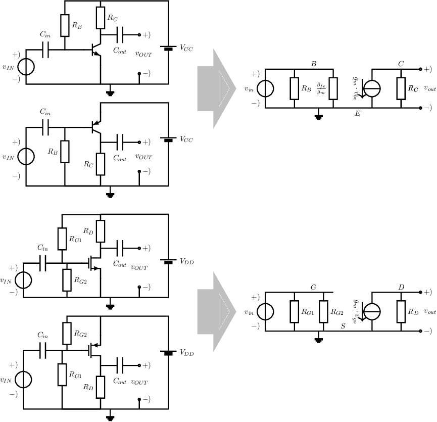
In chapter 4, two simple amplifier circuits were analyzed using small signal equivalent circuits. Figure 4.10 showed a very basic amplifier with one BJT (and its SSEC). In that circuit, the transistor is driven at the port while the output port is between and . This may be somewhat hard to see in the original circuit, but for sure it is very visible in its SSEC. These circuits are both repeated in Figure 5.1 along with their P-type equivalents.
In general a transistor is a three terminal device that behaves like a (nonlinear) voltage controlled current source (VCCS). To be able to behave like a VCCS a device must be at least a two-port device. From a fundamental point of view a two-port device has 4 terminals, whereas a transistor has just 3 which implies that the two ports share one terminal.
For a circuit using a BJT this yields 3 ways to share terminals between input and output port:
All these basic circuits using one BJT have distinct small-signal properties. The figure below lists the 3 possible configurations, starting from the generalized bias circuit for a BJT:
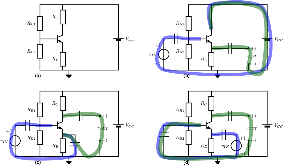
The generalized bias circuit for one BJT is shown in Figure 5.2a. In all circuits either the base or the emitter or both are directly driven by the input signal; driving is done via (DC blocking) capacitances. Drawing one voltage mesh including the input signal and one transistor node pair and drawing one voltage mesh that includes both the output port of the circuit and one transistor node pair directly reveals the common node (in both meshes). In this way Figure 5.2b represents the common-collector circuit (CCC), Figure 5.2c is the common-emitter circuit (CEC) and Figure 5.2d is the common base circuit (CBC).
From the above description, it follows that the bipolar circuits in chapter 4 and the bipolar ones in Figure 5.1 are common-emitter circuits. As these CECs are analyzed in detail in §4.7 no analyses are given (or repeated) here.
The CBC with an NPN is shown in Figure 5.3a; figure 5.3b gives its small-signal equivalent circuit for frequencies where the impedances , and are small enough to be negligible compared to the other impedances. This SSEC is now used to calculate some small-signal properties of the CBC: its input resistance and its output resistance , as well as the small signal voltage gain .

The small-signal input resistance is, by definition, the quotient of and . Using the brute force method, and using a driving voltage source:
Substituting these equations gives for the input resistance:31
| (5.1) |
Equation (5.1) shows that the input resistance of a CBC consists of three components. For decent BJTs, the current gain factor is quite large, resulting in an term that is negligible compared to the term. Using the relation for transconductance of a BJT it follows that for the terms and :
from which we see both terms are identical in size for a DC bias voltage drop across as low as 25 mV. In pretty much all CBC circuits, this voltage drop across is significantly larger — usually at least some tenths of a volt — which gives an input resistance
| (5.2) |
The small-signal voltage transfer is the ratio of voltage variation at the output due to a variation at the input. Again, using the brute force method:
Note that the input and output voltages are in phase, in contrast to the situation for the CEC where the gain is negative and hence the phase difference is (ideally) .
The small-signal output resistance of a circuit can be obtained in a number of ways. For linear circuits (as the SSEC), the three methods which are used most often are:
Note that in the last two methods the input signal source is set to zero. For an input voltage source this translates in effectively shorting the input node in the SSEQ, while for an input current the input current source is to be replaced by an open. Application of the first method, using equation (5.3) gives:
This method requires 2 calculations, while the output of the amplifier at the other two methods is driven with a current or voltage source yielding the output impedance directly. These latter two methods are mostly used in this book.
The CEC and CBC — and their MOS equivalents CSC and CGC — are circuit configurations in which the transistor is driven between base and emitter for the BJT, and between gate and source for the MOS transistors. This nicely complies with the element equation for the two types of transistors where in the normal operating range of the transistors the output current is a function of the input voltage: and .
Another useful configuration is the common-collector circuit where the transistor is not directly driven between B and E or between G and S for MOS transistors. Instead, the transistor is driven at the base (gate) while the emitter (source) voltage is set via () and serves as output voltage. The corresponding circuit schematic of the CCC with an NPN is given in Figure 5.4a.

Feedback from output current to the non-driven input node is typically accomplished by a resistor (or impedance) . The highest attainable value for is using a DC current source instead of .
Using a DC current source, it may be clear that the of the transistor is fixed (assuming no external load and hence zero output currents). Then the difference between the input voltage of the CCC and its output voltage is merely a DC shift. The small-signal value of equals that of and consequently in this case the small-signal gain is exactly one.
Figure 5.4b shows the small signal equivalent circuit, for frequencies where the impedances of the capacitances are negligibly small.
The input resistance Below, the input resistance of the CCC is derived using a driving voltage source. Note that — because of Ohm’s law — we would get a similar expression if we would have used a driving current source. We get:
The equations above are sufficient to calculate everything within this circuit. Since the expression for depends on , we must separate the variables32 , yielding:
After simplification of this relation, we may get (5.4). Note that simplification does not change the relation; it merely changes its form, appearance and its readability. The above derivation would have been shorter using a driving current source.
| (5.4) |
It follows from this relation that the input resistance of the circuit is more or less equal to , parallel to the resistance of the input (bias) circuit: the input resistance of a CCC is usually relatively high.
The small signal voltage gain of the circuit equals the ratio between the small signal output voltage and the (driving) input voltage:
From the relation above, it follows that the small signal voltage gain is smaller than or equal to 1. The gain approaches 1 when either the transconductance or the resistance go to infinity. Note that if a current source would have been used instead of , the signal transfer (without load impedance) is exactly equal to 1. This circuit is commonly called an “emitter-ollower”33 , since the output and input voltages have an equal phase and (almost) equal amplitude.
The output resistance In the derivation of the output resistance shown below, it is (arbitrarily) assumed that the output port is driven by a voltage source. In the derivation, all other independent sources must be set to zero (i.e. ) yielding:
The dominant factor in the expression for is the transconductance of the transistor . As numerical example, a bias current of 1 mA yields a small signal output resistance of less than 25 , which is quite low. Please keep in mind that this impedance is a small signal impedance: the output current should be (sufficiently) smaller than the bias current . In other words: although can be low, the circuit cannot provide significant output currents.
All three variants of the single-BJT amplifier circuits have different small signal properties. Table 1 gives a comparative summary of the results of the three circuits with respect to signal transfer, input and output resistances.
| circuit type | CEC | CBC | CCC |
| transconductance for given | |||
| input resistance |
(average) |
(low) |
(high) |
| signal transfer or voltage gain | |||
| output resistance |
(average) |
(average) |
(low) |
The basic circuits discussed in section 5.1 contain just one transistor. For some applications one of these circuits may do: if the set of small signal properties listed in Table 1 satisfies all your requirements, you’re done.
However, many times none of the basic circuits in section 5.1 can satisfy a set of small signal requirements for a specific application. For example for an audio power amplifier a requirement may be to design a high , a low and a high voltage gain . None of the basic circuits in section 5.1 can achieve all these. The basic circuits can however partially satisfy the requirements, see Table 1. The fact that the basic circuits can in general not satisfy an arbitrary set of requirements is a direct consequence of the limited number of degrees of freedom in circuits with just one transistor. If we must satisfy multiple requirements — that are not compatible with any of the basic amplifier circuit — clearly more degrees of freedom must be created. In this chapter this is accomplished by mix-and-match of basic amplifiers into a larger amplifier. In chapter ?? this is extended to opamp-style circuits. As stated, in this section it is mix-and-match.
If a specific set of specifications must be met by a circuit — hereby an amplifier — that can only partially be met by any of the basic circuits in section 5.1, a combination of basic circuits just may do the job. For example, if for an amplifier circuit
is required then — assuming an amplifier with BJTs — the
From this it follows that all demands can be satisfied by cascading basic amplifier stages. Possible implementations that can be designed to meet all requirements include a CEC+CCC cascade (using two stages of amplifiers), and a CCC+CEC+CCC cascade, or a CEC+CBC+CCC cascade, or ... These latter three stage amplifiers can obviously achieve a higher overall voltage gain.
The next figure shows a linear model of a capacitively coupled two-stage amplifier. The amplifier stages are reduced to their bare essence: only the most important parameters are included: the input impedance, output impedance and voltage gain or transconductance34 .
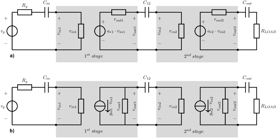
In the representation of a general two-stage amplifier, at both the input and output of each stage a coupling capacitor is included to avoid any possibility for clashing (DC) bias settings. This is however not always required: some basic amplifier stages can directly be coupled which may have advantages for bandwidth, power dissipation and (obviously) component count.
In calculating or deriving the overall properties of cascaded amplifiers, both the properties of the amplifiers themselves and the (signal transfer) effect of coupling needs to be taken into account. A few topics related to this are addressed below. Note that these (small signal) representations are heavily simplified: the input and output impedance of each stage is assumed to be resistive and the reverse isolation — the impact of the signals at the output port on the input port — is assumed to be zero.
Any coupling capacitor in combination with a resistive signal source or resistive load introduces a bandwidth limitation for the signal transfer. In the circuit representations in Figure 5.5 this holds for , and . The voltage signal transfer from to the actual input voltage as experienced by the first stage, , and from input voltage of a stage to its (loaded) output voltage are shown below, as is the overall transfer.
All signal transfers show a high-pass characteristic: the voltage gain is 0 for , while it has a constant non-zero value for . Characteristic parameters for a high pass filter are the “high frequency” signal transfer and the corner frequency:
Note that a voltage-voltage signal transfer is assumed. Getting the signal transfer for e.g. amplifier stages with a current-to-voltage signal transfer is straightforward. For all of these, the corner frequency is identical to the one derived above which can readily be seen using Norton-Thévenin equivalents. The actual transfer function is a little different but can be derived straightforwardly.
Above, an expression for the minimum attenuation when coupling amplifier stages, , is shown when assuming both a source voltage and targeting an input voltage into the amplifier. The expressions for are however different if this voltage-to-voltage transfer is not assumed. For example for an input current-to-voltage transfer and for an input voltage-to-current transfer . For maximum gain it can readily be derived that
The most important property of a voltage source is its low output resistance. From table 1 it follows that the emitter-follower (CCC) and source-follower (CDC) are the closest to a voltage source: they have the lowest of all basic amplifiers. Drive these circuits with a voltage source having a source resistance , then output resistance of the CCC and CDC is
For both the CCC and the CDC, as a decent pessimistic approximation of the output resistance is then . The circuit schematics below show such voltage source circuits, without coupling capacitors to be able to provide DC-voltages. Note that the resistors connecting to the base and gate are not required, but left here only to show the correspondence to the previously used CCCs and CDCs.

It may be clear that (large signal wise) respectively for these two circuits: there is a bias current dependent difference between and and there is a load current-dependent voltage difference. For this translates into the forenamed small signal output resistance . Note that the circuits can source () currents that are substantially larger than the bias current, wile they cannot sink () currents larger than the bias current.
The offset-issue and the limited output resistance (for ) can both be solved by applying feedback. This may lead to e.g. the following circuit schematics. The fact that this circuit cannot sink (significant) currents can be solved by adding its P-type complement.

An ideal current source has an infinite output resistance. A good starting point for the design of a real current source would be a basic circuit that already has a relatively high output resistance: a CEC with emitter degeneration or a CSC with source degeneration. To derive equations for output resistance, we must take the output resistance of the transistor, into account.

The bias current for both circuits in the figure is determined by the (impedance of the) bias source at the input, the degeneration resistor and the characteristics of the transistor. For a current source, this current has to be as constant as possible: the output resistance must be as large as possible. Using the SSEC it can be derived that (for the BJT case):
The output resistance of the circuit is the sum of the output resistance of the transistor and the multiplied degeneration resistor (for the NMOS-version you can set ). Pretty much the same as for the voltage source circuitry in §5.3.1, addition of a feedback loop with an opamp can significantly increase the output impedance.
For a number of applications (in circuits) a sort of copy-circuit comes in handy, for example for re-using or distributing signals or bias settings. For copying a voltage, we can use a unity voltage gain voltage buffer35. To get multiple copies of a specific DC current, multiple current sources as described in section 5.3.2 may be used. In this case, the voltage source may be re-used to drive multiple current source circuits which pushes down circuit complexity.
Another very useful circuit is one that makes an actual copy from some input current. Noting that the current-voltage relation of a transistor is monotonous, a convenient method to achieve this is:
A number of circuit that implement this is shown below; in these circuit schematics, it is assumed that the output current can flow into some node. These circuits are called current mirrors .

Again, the value of the degeneration resistance can be chosen freely: they influence both the output resistance and the required voltage headroom. Obviously, we can also create current mirrors with PMOS transistors and PNPs. Even more so, any active element with an arbitrary monotone function between output current and input voltage will do for a current mirror. A number of characteristics of current mirrors are calculated below.
The small signal current transfer can be derived from a small-signal equivalent circuit of third current mirror, neglecting the transistor’s output resistance:
If both transistors are identical, with the same and , then the relation simplifies to
For the large signal current transfer:
Yet again, this is an ugly bugger, though the large-signal current transfer is linear because the nonlinear element equation for the BJT is used in combination with its inverse. This equation can be simplified further if we assume identical transistors:
This result can also readily be derived noting that for identical BJTs operated on the same the collector currents are equal. Noting that the input current consists of the collector current and two base currents whereas the output current is only the collector current leads to . For unequal transistors, we get a non-unity current gain factor; this can be very useful in some circuits.