13 High-frequency effects in real circuits
If the physical size of a circuit is much smaller then the wavelength of signals in that circuit, the wave-like nature and the finite speed
of an EM-wave does not really have to be taken into account. In that case Kirchhoff’s voltage and current laws can be applied. For
example, for an audio amplifier operating up to (let’s say) 20 kHz, assuming that the speed of an EM-wave in a metal is about 2/3 of
its speed in vacuum, the wavelength of an EM-wave is about 10 km. Any audio amplifier that is orders of magnitude
smaller than that can very well be described and analyzed using the (quasi static) Kirchhoff voltage and current
law.
13.1 A single wire
At very low frequencies a wire simply behaves like a short or a low-ohmic resistor. At radio frequencies (RF) this is
not the case any more, due to the sheer length of a wire and the finite speed of an EM-wave passing through the
wire. There are many models that describe the series inductance associated with wires at RF; one of the more
simple ones being the following which is valid for a round wire that is far away from any return ground path [18, 19]:
|
| (13.1) |
where is the wire
length in cm, and
is the wire diameter in cm.
This translates into — as a rule of thumb — 1 nH/mm wire length. Usually this amount of self inductance is not that relevant at low
frequencies and/or for very short wires, but it may be very harmful already at circuits operating at 100 MHz with wires that are longer
than a few mm. Wires with other shapes or wires that are relatively close to other conductors exhibit a different relation with wire
length.
As example for the impact of a wire, let’s consider a capacitor including wires.
Wires translate into series inductance.
The total impedance of the
capacitor including wires
is then:
Which can be used to derive an equation for the equivalent capacitance
for the
original capacitor including wires. This equation is very much (angular) frequency dependent:
Aiming at (arbitrarily) an impedance of ,
to be used in an oscillator, ideally the capacitance value is
- at
the corresponding capacitive value is ,
and 1 cm wires would add a total series inductance equal to
which corresponds to a series impedance of about
which is negligible compared to the impedance of the capacitor.
- at
the corresponding capacitive value is ,
and 1 cm wires add a series impedance of about
which is small compared to the impedance of the capacitor.
- at
the corresponding capacitive value is .
Having wires of 1 cm add a series impedance of about
which does impact on the net capacitor value. Now .
Note that the wires serve to increase the (equivalent) capacitance.
- at
the corresponding capacitive value is ,
and 1 cm wire adds about .
Then the total impedance of the capacitor including 1 cm wires turns out to be inductive. Clearly using this capacitor
including wires as ”C” in an LC-oscillator will not lead to oscillation.
Note that the impact of wires, for a capacitor, is very dependent on both the capacitive value and on the frequency. For example, for a 1 nF capacitor with
2x1.5 mm wires at 100 MHz
while somewhat longer wires result in inductive behavior at that frequency.
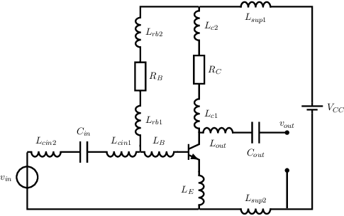
Example As example of the impact of wire length on circuit performance, a quite straight forward common emitter circuit is used.
Assuming 5 mm long wires for /textitevery connection, the following circuit is obtained.
A common-emitter amplifier with wires modelled.
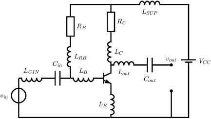
After
some simplifications — merging inductances in series — this simplifies to the following circuit. Note that for biasing, the presence of
the (inductances associated with the) wires does not change anything. However, for sufficiently high signal frequencies the small
signl properties of the circuit may be changed quite a lot. Analyzing/deriving the small signal properties this full circuit is a lot
more work that analyzing the original circuit because of the increase component count and it leads to hard-to-read
relations.
A common-emitter amplifier with wires modelled - with some inductances merged.
Analyzing the impact of each wire-inductance individually is however straight forward, and the resulting
relations are readable and interpretable The impact of the inductances that are in series with the capacitors,
and
is clearly an impedance in series with the input node and output node.. Assuming that
is the
only (significant) wire, and assuming that the impedance of the capacitors is small at signal frequencies, the (magnitude of the)
voltage gain is lowered and the input impedance is increased.
Similarly, assuming that only
has significant inductance, again the input impedance is increased and the (magnitude of the) voltage gain is reduced:
The impact of
on small signal properties is mainly an increase in the amplifier’s input impedance.
mainly
causes an increase of the (magnitude of the unloaded) voltage gain and an increase of the output impedance of the
amplifier:
13.2 Transistor capacitances
Also note that whereas capacitive effects in transistors — such as junction capacitances in BJTs, see e.g. $2.3.2, §2.3.3 and
gate-source and gate-drain capacitances in MOS transistors, see e.g. §2.5 are usually ignored, this may not be allowed towards
higher frequencies. Typically, at RF these capacitances must be taken into account, which makes circuit design or circuit
optimization quite a bit more more complex.
13.3 Two parallel wires - transmission line
Similar to the single wire case described above, two parallel wires also have self inductance. Because these two wires “see” each other the
relation between self inductance and geometric parameters is a little different [18, 19, 20]. Denoting the distance between the wires as
and again denoting
the wire thickness as ,
for
Being two parallel conductors, there is also a capacitance between these two wires. Again assuming for
, the
relation between capacitance and geometric parameters is
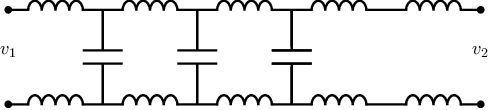
From this, two parallel wires can be modelled using (many physically short) sections that have series inductance and parallel
capacitance.
Two parallel wires: a lumped L-C network, forming a transmission line.
Looking into the pair of wires, this gives rise to an impedance
This means that a signal passing these two parallel wires experience an impedance
while there is
no (NO!) dissipation as there are only inductances and capacitances involved. The impedance only means that there is a ratio between
voltage and current when the signal passes through the two parallel wires; this impedance is typically denoted as the characteristic
impedance of
the pair of wires. Two-parallel-wire configurations are denoted as transmission lines as signals are transmitted through these.
One well known variant of two-wires transmission lines is the “wire over plane” construction. Using symmetry,
is can readily be derived (just slide a ground plane in the symmetry plane between the two wires) that then the
capacitance (per unit length) is doubled and that inductance (per unit length) is halved,, still using the (now
imaginary) distance between the original 2 wires. Denoting the distance between the wire and the plane as
this leads
to
Another well known variant is the coaxial cable.
13.4 Reflections
If the wavelength of EM-signals is not much bigger than the physical size of components, wires, ..., then reflections occur at any
impedance step experienced by a signal. For electrical signals this might at first seem quite strange, but it is simply the same
behavior underlying reflections, transmission and more in visible light that happens at a discontinuity in refractive index - you see and
experience it every day. This refractive index is nothing more or less than an impedance change for the part of the EM-spectrum that
we call light.
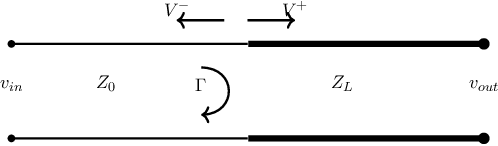
Reflections: part of an incident signal is reflected at an impedance discontinuity.
Without digging into details, part of an incident (voltage) wave on an impedance discontinuity is reflected. The reflected fraction is denoted by the (complex)
reflection coefficient that depends
on the source impedance
and the load impedance
as
The part of the (voltage) wave that is transmitted across the impedance discontinuity can similarly be described by a transmission
coefficient as
described below. This has similarities with the theorem on maximum power transfer but it is fundamentally different as this
and
deal with
the reflected wave behavior of EM-waves.
13.5 Maximum power versus maximum power transfer
A recap of maximum power transfer and the associated conjungate impedance matching was
presented in section 0.21. This assumes an equation for power ending up in a load impedance
, for a source with
source impedance and
a voltage amplitude
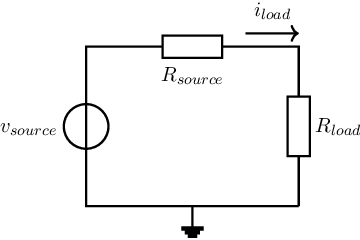
for the configuration in the figure below.
The maximum power as a function of
can be obtained via differentiation:
This directly shows that the power in the load is at its maximum if the load resistance is equal to the source resistance:
.
In a similar fashion, we find that the power transfer with complex impedances is highest for
. A fairly
simple result that you can use to design a load. At the same time, you should not use this when designing a power amplifier, or when
having voltage or current limitations in the driving power source.
An amplifier (modelled by the voltage source and its output resistor ) with a load
The optimum above holds for the case when you assume an ideal source with a certain — fixed — source impedance, which does
not apply if you design your own power amplifier. If you design an amplifier, then you have to deal with limitations in output voltage
and output current, and you have a degree of freedom in the output impedance of your amplifier. If you want a maximum output
power, then you have to take these conditions into account.
Assuming an ideal voltage source, without any voltage limitation and without current limitation, the power into the load not only depends
on but also
depends on and
. Two additional ways
to maximize the power
into
follows from the following two (partial) derivatives:
that show that
- the partial derivative
for every source voltage (amplitude) and combination of resistors. Hence, to obtain maximum ,
the output impedance of the amplifier
must be as low as possible.
- the partial derivative ,
from which it follows that for maximum
the voltage (amplitude)
must be as large as possible,
In case you design an amplifier, the output impedance
is designed by you, the circuit designer. The second item is usually limited by things like (clipping to) a given supply voltage. As long
as no clipping occurs — in voltage or current — the system is perfectly linear and for maximum power into the load, you can
minimize the output impedance of the driver/amplifier, maximize the signal swing and use (conjungate) matched
load.
Actual drivers/amplifiers always have limitations in output voltage (amplitude) and in output current (amplitude). This is straight
forward implication of using non-linear components such as transistors. The current limitation and voltage limitation are
properties of (the design of) your circuit and these limitations are usually fairly independent of the load impedance
. With
current or voltage limitations, (13.2) does not hold and consequently (13.2) (13.2) nor (13.2) are not valid.
Maximum power into
is now obtained:
- achieving maximum
when driving
- having minimum ,
for maximum
and driving
Note that to achieve maximum :
-
when designing a driver/amplifier and having a fixed ,
the output voltage amplitude
must be maximum and
should be minimum and the maximum output current amplitude must be (at least)
|
|
-
when designing the load ,
the amplifier should be loaded in such a way that maximum output voltage amplitude
and maximum output
current amplitude
are achieved at the same time. Then [21],
|
|
Note that this is quite different from the condition of maximum power transfer following from (13.2) and recapped in
section 0.21. This is because the derivations above are for maximum power. And more power is more better.
In actual RF power amplifiers, the load impedance that results in maximum power is more complex. The conventional way to estimate this
is to
apply a variable load impedance (variable real and variable reactive part) and sweep both while monitoring the real power. This
approach is called a load-pull measurement or simulation; a good intro is described in [21]. This also shows that conjungate
matching is not applied to get maximum power which should be obvious when assuming ideal (but current limited) voltage sources
or ideal (but voltage limited) current sources.
Wave-behavior of the RF-signals only kick in if lengths (of e.g. wires, cables, transmission lines, components) are significant
compared to the wavelength of the signals. Then reflections as described in §13.4 become relevant and impedance matching should
be done to get maximum power in your load. However, do not impedance match directly at the output of an RF amplifier if you want
maximum power.