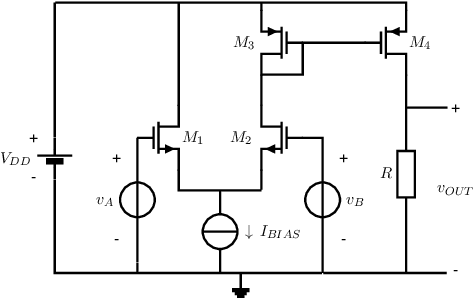
Exercise 8.11 An opamp circuit schematic
In the opamp circuit schematic shown below, all NMOS transistors are equal and all
PMOS transistors are equal. For all transistors you may assume the square law:
.

-
a)
- Derive the bias currents for all transistors in this circuit schematic, for .
-
b)
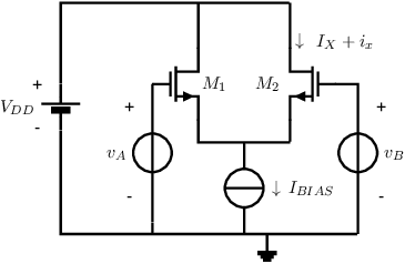
- The op amp has a differential input stage as indicated below, where the drain current of
is used as output current. Give an expression for the small-signal transfer function from the
differential input voltage ()
to ,
as a function of
and the transistor parameters
and/or .

-
c)
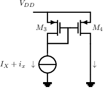
- The output current of the differential pair is fed to a current mirror as indicated below. Give an
expression for the total output current of the current mirror, i.e. the drain current of .

-
d)
- The output current of the current mirror flows into a resistor with value .
Derive an expression for the voltage across the resistor as a function of
and .
-
e)
- Derive an expression for the small-signal voltage gain of this op amp .
