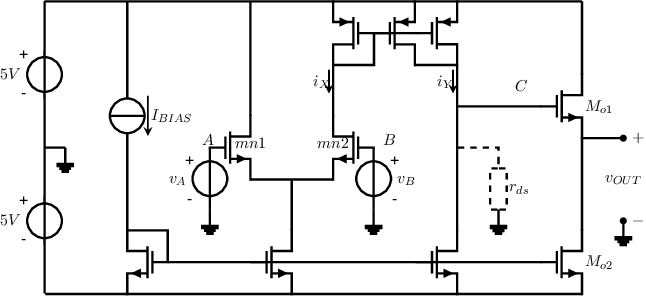
Exercise 8.12 A more elaborate opamp circuit schematic
The figure below shows the circuit schematic of an op amp. For the NMOS transistors
while for the
PMOS transistors ;
all transistors can be assumed to operate in strong inversion, saturation: there the square law
()
holds.
The two output transistors
and are equal, with
. All other NMOS transistors are
also equal, with , and the PMOS
transistors are the same with .
The current source
is . The dashed
resistor
indicates the combined small-signal drain-source resistance of the 3 transistors connected with their drain to
node .

-
a)
- Derive the bias currents in all transistors, for ,
expressed in .
-
b)
- Which input is the non-inverting input and which input is the inverting input?
-
c)
- Give an expression for the small-signal output resistance
of this opamp.
-
d)
- Calculate the required value for
of the output transistors so that the output resistance .
-
e)
- Derive an expression for the small-signal transfer function of the differential pair, from ()
to .
After that, express this also as a function of e.g. ,
,
,
.
-
f)
- Derive an expression for the small-signal transfer function from
to ,
as a function of e.g. ,
,
,
.
-
g)
- Derive an expression for the small-signal transfer function from
to the voltage at node ,
as a function of e.g. ,
,
,
.
-
h)
- Derive an expression for the small-signal transfer function from the voltage at node
to the output voltage ,
as a function of e.g. ,
,
,
.
-
i)
- Derive an expression for the total small-signal voltage gain of this opamp ,
as a function of e.g. ,
,
,
.

