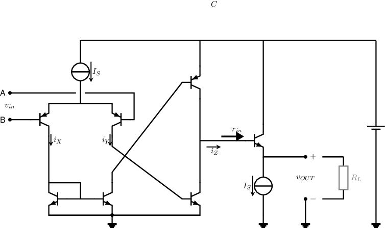
Exercise 8.10 An opamp circuit schematics
The figure below shows the circuit schematic of an opamp. All BJTs have the same (absolute value of)
, have
identical
and .
Furthermore,
as the circuit operates at room temperature.

-
a)
- Which one of the inputs is the non-inverting input?
-
b)
- Derive an expression for the small-signal transfer function of the differential pair .
-
c)
- Derive an expression for the differential input resistance of the opamp.
-
d)
- Derive an expression for the small-signal current
due to
and due to .
Note that this leads to 2 current transfer functions
and .
-
e)
- From the derivations to a previous question, it appeared that .
Now, derive the current transfer from the differential current
to
-
f)
- Derive an expression for the input resistance
of the output BJT, including the load resistor .
-
g)
- Derive an expression for the input resistance
of the output BJT, for an unloaded opamp which is equivalent to .
-
h)
- Derive an expression for the small-signal voltage gain from the voltage at the base of the
rightmost transistor to the output, again including the load resistor .
-
i)
- Derive an expression for the output resistance of this opamp (this expression does not contain
).
Given is that .
-
j)
- Calculate the voltage gain of the total opamp, from
to ,
for .

