Exercise 5.5 A common-base and a common emitter amplifier
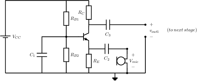
The figure below shows the circuit schematic of the input stage of a low-noise
dynamic microphone pre-amplifier. The voltage from the microphone is indicated by
. In this circuit, the supply
voltage . The transistor has a
very large output resistance and .
For the signal frequencies of interest all capacitors may be considered as low-ohmic.

-
a)
- Derive that the voltage gain
of this circuit is ideally given by
if there is no load connected to the output of the amplifier.
-
b)
- In reality, the circuit will be loaded by the input impedance of the next (amplifier) stage. Draw the
small signal equivalent circuit, including the input resistance
of the next amplifier stage
-
c)
- Derive an expression for the voltage gain
of the input stage, loaded by the input resistance
of the next stage.
-
d)
- Derive an expression for the input resistance of the pre-amplifier input stage.
-
e)
- Calculate the required bias collector current
for an input resistance of
(apparently the optimum value for the selected microphone).
-
f)
- We assume for now that
of the next stage is .
Derive an equation for
to obtain a voltage gain
of the input stage.
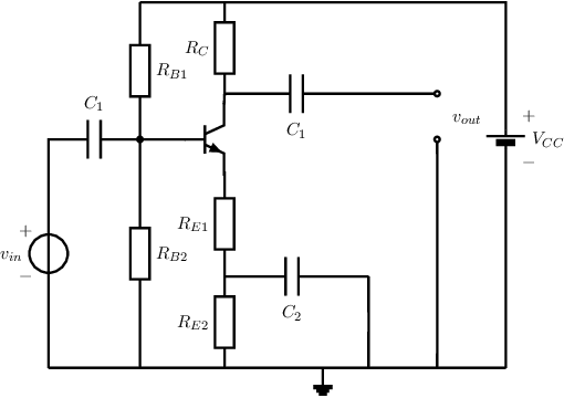
The following figure shows the schematic of a second amplifier stage that is used to further
amplify the voltage from the input stage reported above. To reduce the distortion due to the
relatively large signal levels, emitter degeneration is used via resistor .
Again, ,
,
and for the signal frequencies of interest all capacitors may be considered as low-ohmic.

-
g)
- Draw the small signal equivalent circuit for this second amplifier stage.
-
h)
- Derive an expression for the voltage gain of this second amplifier stage.
-
i)
- Derive an expression for the small-signal input resistance
of the second amplifier stage.
-
j)
- The second amplifier stage is dimensioned as follows: ,
,
,
,
.
Calculate the numerical value of the input resistance of the second amplifier stage. Is it smaller
or larger than the assumption of ?
How does this affect the voltage gain of the input stage?
