In stable systems, the loop gain does not encircle the point “-1” in the complex plane in the clockwise These stable systems are usually linear, except when explicitly using non-linear components or when running into some limit like clipping to the voltage supply. Because these systems are linear(-ish),:
If the “-1” point in the complex plane is encircled in the clockwise direction by the loop gain , then that system is unstable. Such an unstable system may be in a meta-stable state or it goes to or stays in either of the extreme states — possibly periodically changing its state. Usually these extreme states correspond to an output voltage equal to the positive or negative supply voltage. Theoretically a system can stay in a meta stable point indefinitely48 ; in actual circuits any disturbance (noise, interference, birds flying by) will make the system leave the meta-stable point and go to either of the stable extreme states. These fundamentally unstable systems behave non-linearly and hence cannot be analyzed in frequency domain: they can only be analyzed in time domain. As interesting and as useful as they may be, we’re not going to analyze, introduce or show these unstable circuits49 .
Exactly between the stable systems and the unstable systems are systems for which the loop gain crosses the –1 point in the Nyquist plot. Systems for which the loop gain curve crosses the “-1” point will be shown to oscillate harmonically (sinusoidal) at the frequency corresponding at which the Nyquist plot crosses that – 1 point.
Harmonic oscillators are systems for which the Nyquist plot crosses the “” point for one specific (non-zero, finite) frequency. The hows and whys for this are briefly introduced below. After that, a variety of harmonic oscillators are discussed. Although the basics are identical, the actual circuit implementation of oscillators can be very different, all with their specific advantages and disadvantages.
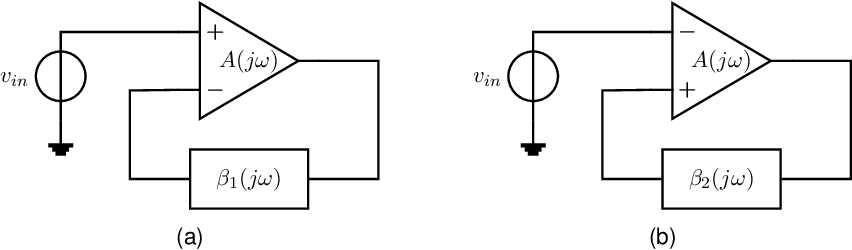
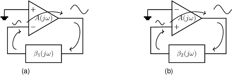
As starting point, let’s assumed the negative feedback configuration shown in Figure 8.1a, having a forward gain and feedback gain . Using this configuration, it will be shown that harmonic oscillators can be constructed by ensuring that the Nyquist factor . for one specific non-zero and finite frequency . Originally the Nyquist factor is defined as , for a negative feedback to (hence) the inverting input of the amplifier as shown in Figure 8.1a. This negative feedback arrangement is common practice for amplifier circuits and other stable systems, but it is not necessary for oscillator circuits.
Harmonic oscillators from systems with negative feedback
The signal transfer – or closed loop gain – of the system with negative feedback in Figure 8.1a, is
Assuming that the Nyquist plot crosses the –1-point, for the specific (radian) frequency where the Nyquist curve actually crosses the –1-point, the denominator of the closed loop transfer function of the inverting configuration in Figure 8.1a is zero. The transfer for that frequency then goes to infinity:
which implies that the circuit can create an output signal with a finite and non-zero magnitude at from nothing. An output signal for one non-zero finite frequency is a harmonic signal (a sine): we have a harmonic oscillator and the circuit consequently behaves as a sine generator. Note that this happens under two very specific conditions that both should be satisfied for the same :
Harmonic oscillators from systems with positive feedback
Stable circuits rarely use positive feedback; for oscillators it can however be useful. Above, is was stated that for an infinite closed loop gain at a single frequency, that system can oscillate harmonically. Assuming the configuration with positive feedback shown in Figure 8.1b, it can readily be derived that the closed loop gain is
This closed loop gain goes to infinity for , for which case harmonic oscillation is achieved at . Compared to the case with feedback to the inverting input of the amplifier, this oscillation condition is different by a factor :
Harmonic oscillators: general formulation
Oscillation requires feedback. As shown above, both systems with feedback to the negative input of an amplifier and systems with feedback to the non-inverting input of an amplifier can be used for harmonic oscillators. In both cases, the total loop gain including any (inversion) sign must equal for one single (non-zero and finite) frequency, to get harmonic oscillation. This condition is usually referred to as the oscillation condition or Barkhausen’s stability criterion.
The Nyquist plot nicely shows (the degree of) stability for systems where the feedback is explicitly to the inverting input of the amplifier. The condition for stability is then that the –1-point is not net encircled in a clockwise direction by the Nyquist contour. This Nyquist contour starts at , goes to and thereafter goes via back to .
Oscillators must oscillate in a stable manner; according to feedback theory that does not corresponds to a stable circuit. Moreover, whereas the Nyquist contour and the Nyquist criterion for stability assumes feedback to the inverting input of an amplifier, for oscillators there is no need to assume negative or positive feedback: only the Barkhausen-criterion must be satisfied. This Barkhausen-criterion states that for one specific frequency. For that reason, in this chapter, typically the loop gain is plotted across all positive frequencies in a polar plot. This typically looks like a -rotated version of (half) the Nyquist plot, where that is due to explicitly including the “-1” of an inverting amplifier input in the loop gain.
To make the loop gain curve cross the “” point in a polar plot, we need an amplifier and a suitable feedback circuit that combined yield a suitable . Many variations on this are possible that each neatly oscillates at a specific frequency. Within this book, we categorize these oscillators based on the so-called quality factor . The quality factor of a system is a measure for the loss of energy during one oscillation period. The definition of the quality factor is
where the term is the total energy within the oscillator and the dissipated power in one period; the is the oscillation (angular) frequency. This relation can be rewritten into an equation relating the total energy in the oscillator and the decrease in energy per oscillation period:
A higher value of corresponds to less energy loss per oscillation cycle which usually translates into relatively power efficient oscillators. These are also (for the same reason) the preferred harmonic oscillators for generating sine waves at high frequencies. Alternatively, low-Q harmonic oscillators are relatively power hungry but typically have advantages in terms of tunability. Low-Q oscillators are covered in this chapter while high-Q oscillators are covered in chapter 9.
Harmonic oscillators with a low quality factor dissipate a relatively large amount of energy per oscillation period. Because of this dissipation, the circuit must, by definition, contain dissipating components: resistors. A number of implementations of these harmonic oscillators, on a high level and assuming one amplifier with frequency independent gain , is given in Figure 8.2.
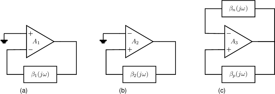
Assuming the amplifier to be ideal (for simplicity reasons), with a frequency independent gain , infinite input impedance and zero output impedance, then the feedback circuit must ensure there is only one non-zero finite frequency for which the loop gain is exactly 1. Hence, the circuit must have a frequency-dependent transfer function. For the three oscillator concepts in Figure 8.2:
feedback to the -input as shown in Figure 8.2a:
for harmonic oscillation, the total loop gain is at only the oscillation frequency. Assuming a constant real and positive then at oscillation frequency the phase shift of the feedback network equals . To accomplish this kind of phase shift at least a third order feedback circuit50 should be used.
feedback to the -input as shown in Figure 8.2b:
the total loop gain is , which equals 1 for one frequency to achieve harmonic oscillation. The phase shift of for this frequency is . To create a frequency-dependent circuit with a phase shift of at only one (angular) frequency, we need a second or higher-order circuit.
feedback to both inputs as shown in Figure 8.2c:
The total loop gain is now just somewhat harder to get due to having 2 feedback paths: it is . For harmonic oscillation this total loop transfer equals 1 for only the oscillation frequency. Again, this requires at least a second-order circuit. This at-least-second-order signal transfer may of course be distributed over and .
All these principles, concerning harmonic oscillators with a low Q, can be found in many examples in literature or in any old stow away box with electronic junk. A few interesting harmonic oscillators with low Q will now be discussed.
A well known implementation of a harmonic oscillator which uses the principle of Figure 8.2b — feedback to the non-inverting input node of an amplifier — is the so-called Wien bridge oscillator. The original circuit is given in Figure 8.3 and originates from bridge measurement equipment.
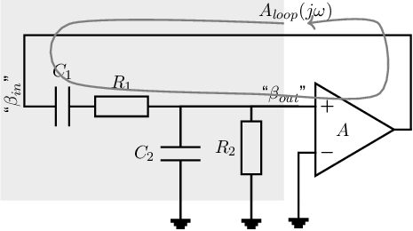
This oscillator circuit schematic may be viewed as an amplifier (with gain ) and a feedback network implemented by the resistors and capacitors. For oscillators, only the loop gain is important and splitting up this loop gain in forward and feedback gain is not required although it may be done intuitively.
In this specific case it may seem natural to split the loop gain into an explicit feedback path formed by the circuitry in the gray rectangle and into an amplification part. Then the input of the network is connected to the output of the amplifier, while the output of the network is connected to the non-inverting input of the amplifier. The signal transfer of the hereby defined -network in the Wien bridge oscillator in Figure 8.3 is then:
The oscillation condition states that harmonic oscillation occurs if for one specific finite non-zero :
Equating the loop transfer to 1 yields two expression/conditions because the loop gain is complex (with a real part and a complex part that both yield one equation). The oscillation frequency follows from equating the total loop transfer to be real (with a zero complex part). The required voltage amplifier gain follows from equating the loop gain magnitude to 1 at . For the Wien bridge oscillator:
Assuming a real valued amplifier gain , the numerator of the loop gain for this specific circuit is real valued. To get a real valued loop gain, then also the denominator of the loop gain must be real valued. Being a complex number for this specific circuit, the upper condition can then be rewritten into
after which the condition — at — can be solved, yielding
This Wien bridge oscillator circuit will hence oscillate harmonically at the (radian) frequency given in (8.3) with amplifier gain as given in (8.4).
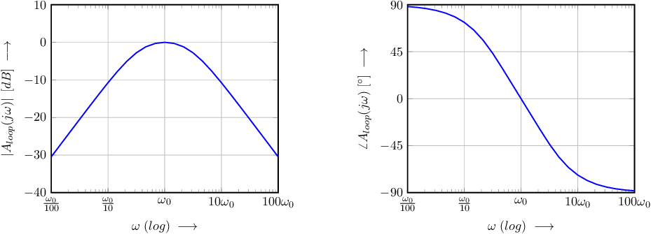
In the derivation shown above, no attempt was made to (re)write the loop transfer into a standard form. Although rewriting does not change anything with respect to the result, the derivation would be a little different. A nice thing about rewriting into a standard form is that a Bode graph is readily constructed. The loop gain in (8.2) can be rewritten into
The follows from making a real value. Noting that the numerator now (due to rewriting) is imaginary, this corresponds to setting the real part of the denominator to zero. yielding (8.3). For this specific , the required amplifier gain is then readily obtained as (8.4). Assuming that and that for simplicity reasons, the resulting loop gain as a function of frequency, yielding oscillation at , is then
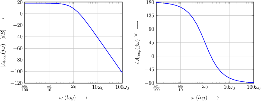
The Bode plot of this loop gain is shown in Figure 8.4, where .
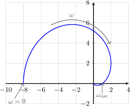
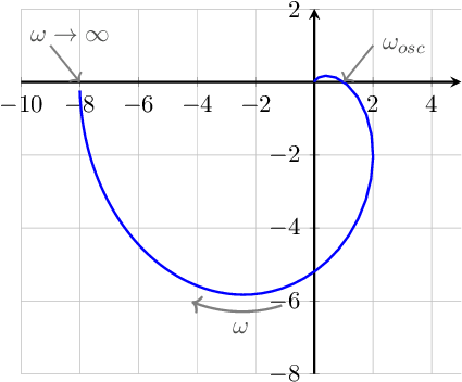
The corresponding polar plot of the loop gain is shown below. In this polar plot, both the direction along the curve, for increasing and a few relevant (radian) frequencies are indicated.
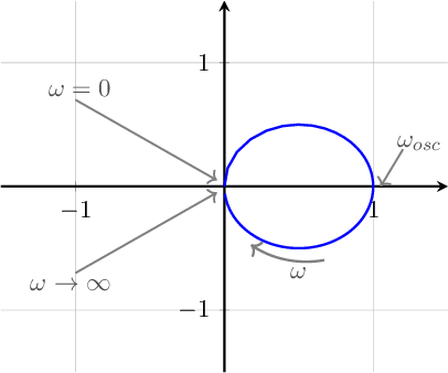
Figure 8.6 shows a few alternative oscillator circuits using a variant of the “Wien bridge circuit”. All of these are combinations of a high-pass and a low-pass configuration to get zero phase shift at the oscillation frequency.
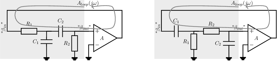
More variants can be constructed, especially if also inductors are included. Similar oscillators with feedback to both the inverting and non-inverting input of the amplifier can also be constructed. The approach to get any circuit to oscillate is however the same: derive the loop gain, equate that to unity for one single finite and non-zero frequency. Equating yields 2 equation, where setting the loop gain to a real value yields/sets the oscillation frequency and thereafter setting the magnitude of the loop gain at the oscillation frequency to unity sets the required gain factor for the amplifier.
Harmonic oscillators that use the inverting amplifier configuration shown in Figure 8.2a are usually so-called phase-shift oscillators. For these oscillators the total loop transfer equals unity at one specific finite and non-zero oscillation frequency. Splitting the oscillator into a forward and feedback gain (again: not necessary as only the total loop gain is important!):
Three stage low pass phase shift oscillator
The simplest form of an oscillator circuit conform the setup in Figure 8.2a is given in Figure 8.7. This circuit schematic includes an inverting amplifier and a frequency dependent part consisting of 3 first order low pass RC sections. For this frequency dependent part, the phase shift decreases monotonically with increasing frequency, from 0 at DC to at infinitely high frequencies. Using an inverting amplifier, the phase shift of the loop gain varies monotonically between 180 at DC to across frequencies and hence there is one frequency for which the phase shift is .
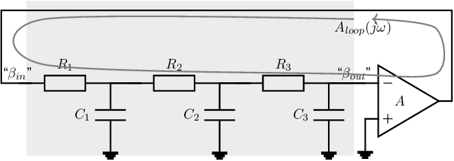
The general transfer function of the circuit in Figure 8.7 cannot be easily derived, since all components influence each other. The calculations are less cumbersome if we assume the RC-members not to influence each other (which is not true in general!). A requirement for this assumption is and . If we then choose , then the loop gain is:
| (8.6) |
To operate as harmonic oscillator, this loop gain must equal (the complex number) 1 for only one frequency. Setting to a real value yields the oscillation frequency. Noting that the numerator of is real, in (8.6) this implies that the denominator at harmonic oscillation also must be real, which is the case for as given by:
At , from which it follows that for stable oscillation the amplifier must have gain . Note that the amplifier is used in an inverting configuration.
The Bode plot of this loop gain is shown in Figure 8.8, where .
The polar plot of the loop gain for this circuit is given in Figure 8.9. Note that this polar plot can (relatively) easily be constructed from the Bode plot of by picking a few sets of and and plotting these along with a smooth connecting curve in a polar plane.
If all 3 resistors have the same value and all the capacitors have the same value, the derivation of oscillation frequency is quite a lot more work. This is because the third RC-section loads the second, that loads the first RC-section. After some work, you can derive that the loop gain equation then is
which yields and .
The oscillator described in the previous section was easy to analyze under assumption that the RC-sections do not (significantly) load each other. That condition was satisfied for and . One way to ensure that RC-sections actually do not load each other is using (ideal) voltage buffers between each RC-section:
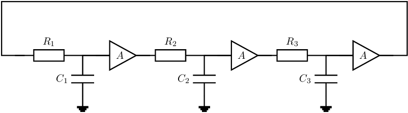
Assuming , the loop gain of this circuit is
The analysis or dimensioning to get harmonic oscillation can be executed the exact same way as for the previously analyzed 3-stage phase shift oscillator.: writing out and equating that to (a complex) 1. Another way is to explicitly leverage the symmetry in the circuit.
The circuit schematic in Figure 8.10 consists of 3 identical parts, that individually consist of an amplifier and an RC-low pass section. For harmonic oscillation,
This translates into the following condition, for harmonic oscillation, for each individual section:
Using an arbitrary amplifier with a positive or negative real voltage gain, and noting that the phase shift of a single first order low pass section is , possible solutions for (8.7) and (8.8) are
assuming :
for :
Note that the “harmonic oscillator” with 3 low pass RC sections and positive amplifier gain “oscillates” at : it yields a DC value. This is usually not regarded as harmonic oscillation. The variant with a negative voltage gain can oscillate at a finite non-zero frequency, for which the (per section) voltage gain is . Being essentially the same harmonic oscillator as in the previous section, the Bode graph and polar plot for the circuit in Fig. 8.10 are also given in Figure 8.8 respectively in Figure 8.9
The 3-stage relaxation oscillators above were implemented with low pass RC-sections. Implementing them with high-pass sections yields the following circuit:
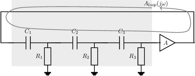
Assuming A0
Assuming a real valued positive voltage gain ,
and assuming that the RC-sections do not load each other, the loop gain is
Defining , the Bode plot of this loop gain is shown in Figure 8.12. It can be seen that the phase condition for harmonic oscillation — — can only be obtained for which is not regarded as an oscillation frequency. Therefore this specific circuit does not implement a harmonic oscillator.
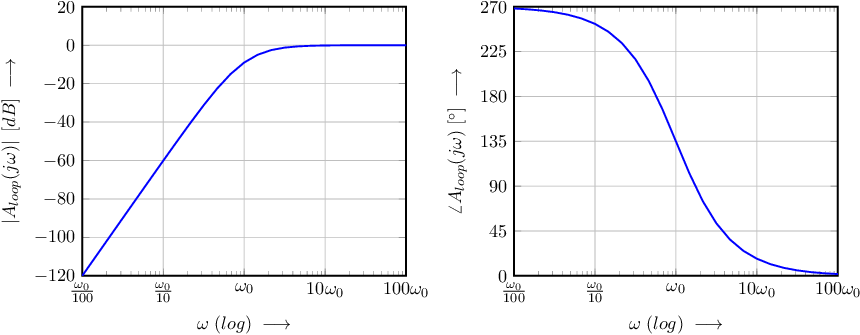
Assuming A0
Assuming a real value negative amplifier gain
and ignoring loading effects of the three RC section (for simplicity reasons), the corresponding
Bode plot is shown in Figure 8.13. The phase condition for the loop gain yields at the oscillation
frequency
For a single first order high pass RC section, the phase shift is between and . From this is can be concluded that the only possible solution for harmonic oscillation is for a phase shift per RC section equal to . This phase shift occurs for . To get the gain of the amplifier then needs to be .
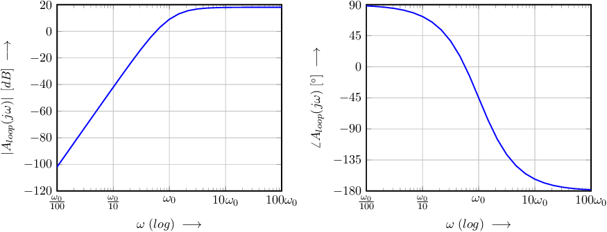
The polar plot of the loop gain for this circuit is given in Figure 8.14.
RC phase shift oscillators with more than 3 stages can be realized. In this section a number of designs are treated briefly. Let’s first assume that low pass sections are used that do not load each other significantly. This can be accomplished by e.g. including voltage buffers between RC-sections or by significantly scaling up the impedance of consecutive RC-sections. Assuming an amplifier with a real negative gain and leveraging the symmetry in the circuit it can readily be derived that:
for the phase shift of the loop gain lies between and , where the originate from the negative real amplifier gain. Denoting the phase shift of the RC-section as , for this situation, oscillation occurs for
for the phase shift of the loop gain lies between and , again with the due to the negative real amplifier gain. Then harmonic oscillation occurs for
for , the loop phase can be for and for . This latter phase shift corresponds to which is not regarded as an oscillation frequency.
for , the loop phase can equal for 2 finite and non-zero (radian) frequencies. For the two solutions it can easily be derived (using symmetry) that both the resulting (radian) frequency and the required loop gain for one solution is (much) higher than that for the other solution:
and
Note that this means that if the circuit is designed to oscillate at , the amplifier gain is set to sustain this oscillation. At the same time, this amplifier gain is (much) to low to sustain the second solution: this second solution will then not yield oscillations.
The other way round, if the circuit is designed to sustain the second solution, for which , the amplifier gain is such that the loop gain at the first solution is much larger than one. The magnitude of that oscillation mode will hence rapidly grow to (theoretically) infinity. This implies that there is no way to get stable harmonic oscillation for the second solution: the first solution will always be stronger.
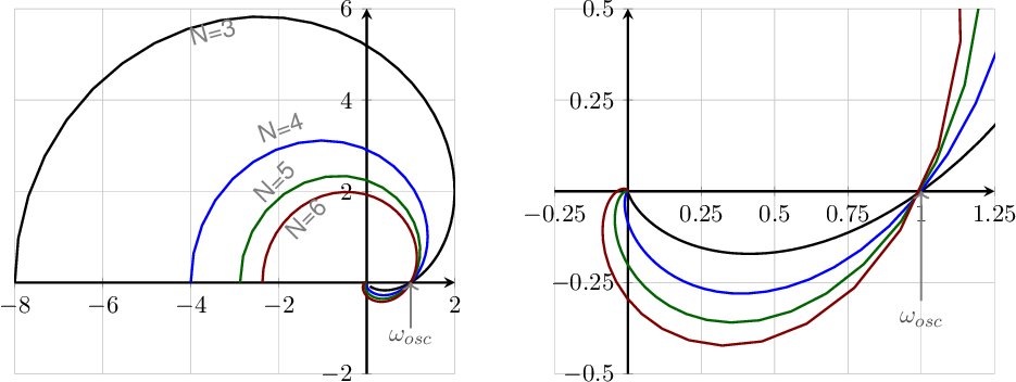
Figure 8.15 shows the polar plots for phase shift oscillators with 3, 4, 5 and 6 low-pass sections. On the left the full polar plot is shown while a zoomed in version is shown on the right hand side. As all circuits are designed to be harmonic oscillators, all curves cross the point. Note that each curve rotates for .
In the previous section, some RC phase shift oscillators with more than 3 stages having amplifiers with negative gain were treated briefly. This specific section shows some ins and outs for low-pass RC phase shift oscillators with positive gain amplifiers.
Let’s first assume that low pass sections are used that do not load each other significantly. This can be accomplished by e.g. including voltage buffers between RC-sections as shown in e.g. Figure 8.10 or by significantly scaling up the impedance of consecutive RC-sections as assumed in section 8.3.3. Assuming an amplifier with a real positive gain and leveraging the symmetry in the circuit it can readily be derived that:
for the phase shift of the loop gain lies between and . For this situation, oscillation may occur for the following two conditions. Note that both conditions do not implement a sensible harmonic oscillator as the oscillation (radian) frequency would be respectively .
for the phase shift of the loop gain lies between and . Then harmonic oscillation may occur for the next two conditions.
The first solution would correspond to oscillating at DC, which usually is not regarded as oscillation. The second solution yields a possible solution for harmonic oscillation at a finite, non-zero frequency.
Trying to get the 5-stage solution to oscillate at will fail. This is because the DC “oscillation” requires a lower gain to achieve “oscillation”. Setting the will result in a very rapidly diverging (to ) output signal for the DC “oscillation” mode.
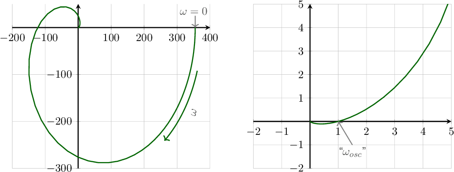
Figure 8.16 shows polar plots of , with and hence dimensioned to oscillate .at The right hand side figure is a zoomed version of the full polar plot on the left hand side. These plots illustrate that although the curve crosses , a real positive exists that causes the previously mentioned divergent behavior.
To analyze a harmonic oscillator (and possibly to dimension that circuit to operate as you want it to operate), an equation for the loop gain of the circuit must be derived. For this, you have to open the loop somewhere, apply an input signal and get the “output signal” of that opened loop.
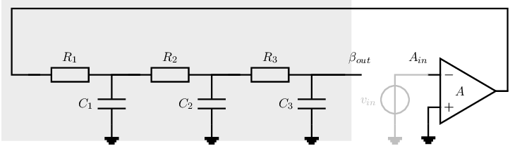
For circuits having an ideal voltage amplifier it may be natural to cut the loop directly in front or directly after the amplifier. From a fundamental point of view, opening the loop and injecting a sine and deriving a proper loop gain requires that:
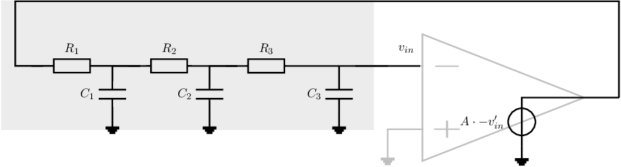
Cutting the loop somewhere in the frequency dependent part of the oscillator circuit schematic (in Figure 8.17 the part in the greyed region) would change impedance levels and therefore would not yield a valid loop gain derivation. For example cutting the loop just after would omit frequency dependency of the combination of and and would change impedance levels “seen” by the rest of the -network as compared to that in the closed loop configuration.
Noting that an ideal voltage amplifier is an ideal two port block consisting of an ideal voltage input port and a voltage controlled voltage source, a generalized guideline is that a loop can safely be opened (for loop gain derivation purposes) inside such an ideal controlled two port component. Then the following configuration is obtained, where the voltage controlled voltage source is driven by and the input signal to this amplifier is , that are equal in the original closed loop configuration
The oscillation condition only gives information on the frequency of the oscillator and conditions for the required gain in the circuit. At a sine at is sustained indefinitely: the amplitude does not grow, nor does the sine die out. Example signals somewhere in an arbitrary harmonic oscillator that oscillates at 10 kHz are shown in Figure 8.19. Both signals are perfectly fine signals at the same node. The two signals differ in signal amplitude by a factor 10.
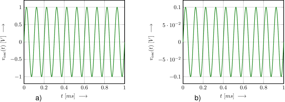
The oscillation condition does not state anything on how the system will start to oscillate nor on the oscillation amplitude. It only states that any signal at the oscillation frequency remains unchanged forever at its initial amplitude. From here, a interesting question arises:
Forcing or designing for a specific oscillation amplitude can be done leveraging the properties of stability (rephrases for harmonic oscillators:
Whereas the constant amplitudes are illustrated in Figure 8.19, the changing amplitudes are illustrated in Figure 8.20.
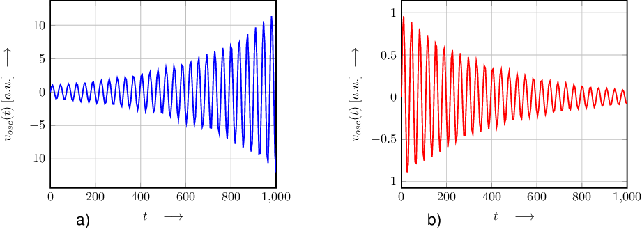
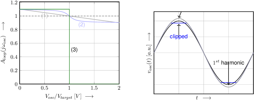
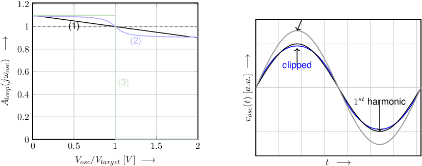
These three types of behavior are used to obtain oscillation at a specific (target) amplitude by ensuring at the target amplitude and having a (slightly) higher or lower loop gain magnitude at respectively a lower and higher amplitude. Three examples of suitable (magnitude of) loopgain at the oscillation frequency are given in Figure 8.21. Note that this does assume a non-zero initial signal in the oscillator; this is addressed in section 8.8.
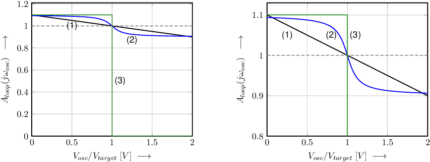
Gain-amplitude curves (1) and (2) in Figure 8.21 can be used both on the signal amplitude and (a bit ugly) on the momentary signal value . If a signal’s amplitude is used to control the loop gain, then a proper estimator for that amplitude is required. This can be e.g. using a peak detector (assuming a sinusoidal signal), using signal power, using a Fourier transform, ... This is worked out a little in §8.6. Working on a momentary signal , all curves implement to some degree (soft or hard) clipping which necessarily distorts the signal(s). Some examples of clipping types of amplitude control are shown in §8.7
An amplitude-dependent gain can be created in a number of ways. Obviously, for every implementation, some kind of amplitude estimator is required. That amplitude information must then be used to control the (amplifier’s) gain in the oscillator circuit. An example is given below, assuming a Wien bridge oscillator. Implementing the amplifier as a non-inverting opamp configuration as discussed in section 7.2.1, adjusting gain can be done by adapting resistor or in its feedback path. If enough power is dissipated in or to cause amplitude-dependent heating, these resistors may be implemented as Positive Temperature Coefficient (PTC) resistor or as Negative Temperature Coefficient (NTC) resistor respectively. The resistance of a PTC resistor increases with temperature. Implementing with a PTC resistor and designing such that a signal amplitude translates in heating the PTC effectively implements an amplitude stabilizing feedback. Implementing as an NTC resistor does the same.
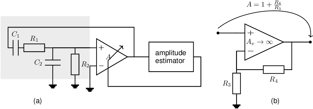
There are many other ways to implement a tunable voltage gain, including making the bias current of the amplifier (or an amplifier stage) dependent on and thereby implementing gains that result in loop gains similar to those in Figure 8.21, curves (1) or (2).
Whereas amplitude control that actually uses amplitude information is the proper way, and yields the most clean signal, it does require a proper estimation of the amplitude and requires a proper way to tune a (linear) gain. A more crude way is to soft or hard limit (clip) a signal. Neglecting some other effects, clipping lowers and limits the harmonic content of the signal at which effectively lowers the loop gain.
This is illustrated for the loopgain-amplitude curves in Figure 8.21.
For very low signal amplitudes, for the curve marked with (3) in Figure 8.21, (replicated below) the oscillation signal amplitudes grows exponentially until the signal amplitude reaches as defined in the same figure.
With increasing amplitude, an increasing part of the signal now gets clipped. This results in a signals as shown in the time-domain figure below. Assuming no clipping, for a signal with amplitude larger than the gray sinusoidal signal would result (indicated by “unclipped”). The actual, clipped, signal is shown in blue and indicated by “clipped”. The frequency component at is shown in black and indicated by “ harmonic”.
For very low signal amplitudes, also for Figure 8.21, curve (1), and the oscillation signal amplitudes grows (not exponentially in time) until the signal amplitude gets close to . Due to the quite smooth “clipping” the resulting signal gets compressed but does not show the nasty distortion as described above:
In a harmonic oscillator, a larger-than-unity loop gain takes care of increasing signal amplitudes. To actually get oscillation, a non-zero initial amplitude at (or close to) the oscillation frequency. This initial amplitude can be ensured in a number of ways:
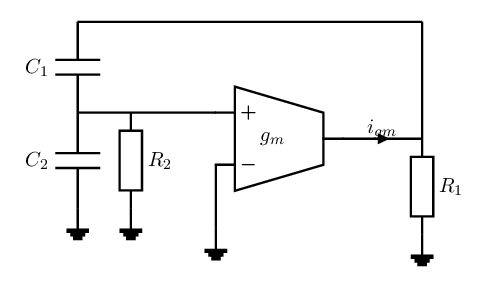
All harmonic oscillators discussed so far in this chapter were built around an ideal voltage amplifier: a block with a frequency-independent voltage gain , an infinite input impedance and a zero output impedance. At higher frequencies, and almost always in integrated circuits, the natural active building block is however not a voltage amplifier but a transconductor, drawn as the -block in the circuits below. A transconductor implements a voltage-controlled current source (VCCS) with as element equation
with — ideally — an infinite input and output impedance. Switching to this building block seems to require a complete redo of all the loop-gain derivations. It does not: the step from a voltage amplifier to a transconductor is nothing more than a Thévenin–Norton transformation, and all results of the previous sections carry over unchanged.
Thévenin–Norton equivalence. With the Thévenin–Norton equivalence, a voltage source that delivers a voltage with series impedance is equivalent to a current source delivering a current with a parallel impedance . The easiest way is however to assume resistive-only impedances. This latter equivalence is depicted in Figure 8.23: a voltage source in series with an impedance is (seen from its output terminals) equivalent to a current source in parallel with that same impedance . This equivalence also holds with voltage-controlled sources, e.g. with a voltage amplifier and a transconductor.
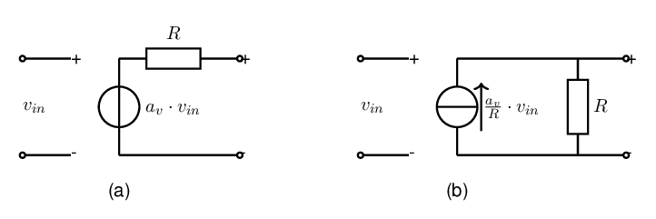
Consequently, in oscillators that include a voltage amplifier with a series
,
these two can conveniently be replaced by a transconductance with a parallel
.
A transconductor can implement a voltage amplifier with . As derived for common drain circuits and common collector configurations, a transconductor in (negative) feedback configuration behaves as a voltage source with an output resistance . In schematic this yields the following equivalence, where (left) the transconductance is represented by its (trapezoidal) circuit symbol. To avoid confusion about the current direction, is explicitly shown.
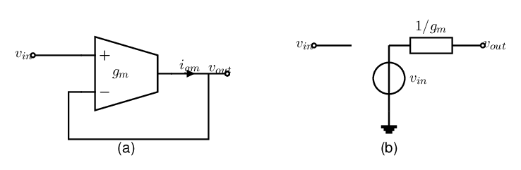
Consequences for the oscillators. With the above explained equivalency, we can simply replace an ideal
voltage amplifier with series resistor by a transconductor that is either in a feedback configuration or that has
a shunt resistor. The loop gain then keeps exactly the same form as before under the substitution
respectively
. As a
result the oscillation frequency — fixed by the frequency-dependent network and not by the amplifier — is
essentially unchanged, and only the amplitude and start-up condition is reinterpreted. Note that with
transconductors in feedback configuration, the equivalent voltage gain is positive.
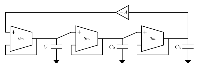
As a first example, Figure 8.25 redraws the Wien bridge oscillator of Figure 8.3 with a transconductor. Because the transconductor delivers a current, the resistor is now placed as a shunt at the transconductor output node. Via the total feedback networks (, , and ) the frequency-selective feedback to the non-inverting input is implemented. The oscillation condition is obtained exactly as before — equate the loop gain to unity for one finite, non-zero frequency — now with in place of .
As next example, the distributed three-stage phase-shift oscillator in Figure 8.10 can be morphed into the transconductor version of Figure 8.26. Each transconductor now drives only a shunt capacitor. The transconductor with negative feedback implements the (positive) voltage gain with output resistance . The three identical – stages behave exactly as the original three buffered RC-stages do. Note that an extra inverting amplifier is required for oscillation at a non-zero frequency51 .