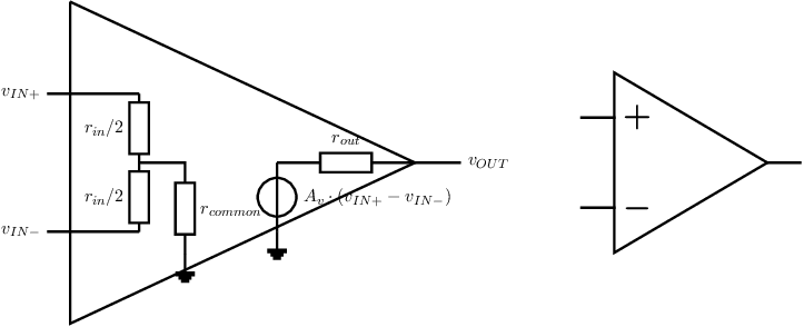
This chapter introduces the operational amplifier, or op-amp, as an abstract electronic component. The internals of opamps will be detailed in chapter ??; This type of amplifier has two characteristics that we already used in feedback systems: it has a subtraction point and a high voltage gain. The term operational amplifier stems from the era where signal conditioning and operations on signals were done only in the analog domain: the 1940’s to 1960’s. Using op-amps many mathematical operations could be implemented wrapping proper feedback circuitry around them. Using op-amps, multipliers, adders, differentiators and more can easily be implemented. Drawbacks of op-amp based signal operations include noise, and spread issues (not addressed in this book), frequency dependencies and impedance related issues. Nowadays signal processing is preferably done in the digital domain, which is more power efficient at low frequencies, does not have impedance or spread related limitations and is quite easy to generate.
Nowadays, op-amp-like configurations — a gain stage with feedback wrapped around it in some way — are still widely used in electronics at all places where digital signal processing cannot be used: in signal conditioning, basic amplifiers, analog-digital conversion, in RF circuitry, in A-D conversions and D-A conversions and more. In this chapter mainly simple applications of op-amps are discussed, along with the major non-idealities and their impact.
The symbol of an op-amp is shown in Figure 7.1: it is essentially a voltage amplifier with a differential input voltage that generates an output voltage . For an ideal op-amp, the voltage gain , the input impedance and the output impedance . The circuitry inside the op-amp is not dealt with in this chapter: it consists of a number of basic building blocks — similar to the ones in chapter 5 with some additional ones, see chapter ?? — that all together make the op-amp.
Op-amp based circuits are frequently used for analog signal processing applications. These mainly include linear processing such as current-to-voltage conversion, voltage gain, filtering, integration and more. In the following subsections a number of these applications are discussed in some detail. Extending it to other signal processing functions is quite straight-forward.
One of the basic configurations of an op-amp is given in Figure 7.2. Negative feedback is wrapped around the op-amp, while the total circuit is driven at the +-input. For clarity, the non-ideal input and output resistance and the voltage controlled voltage source that models the operation of the op-amp are shown in grey. Below, a number of properties for this circuit configuration are derived.
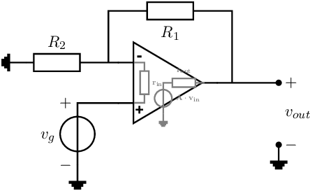
The voltage gain of the circuit above can be easily calculated using some simplifications (idealisations): and . An example of the derivation of the voltage gain is:
The relation for the voltage gain immediately follows:
The input resistance of the circuit can easily be determined. Firstly this input resistance is derived explicitly assuming a finite value for . The hardest part of this is — with the brute force approach — to neatly find all the simple relations iteratively and to keep track of what’s already been described:
Substituting all these relations gives the desired result. Note that the relation for below is rewritten a few times. This does not change the relation: they are identical and hence they all are just as correct as the other. The main purpose however is to get a readable relation:
It looks like a lot of work, and it is. However, if we assume to be much larger than and , then the derivation becomes much more simple:
This relation clearly shows that the input impedance of the non-inverting amplifier configuration is quite high for large values of . The limit, for the input impedance of this system is for any positive : even for e.g. with you will get an infinite system-input resistance.
The output resistance of the circuit is calculated in pretty much the same way as described above. Assuming that the output port of the system is driven by a voltage source — with — and assuming an infinite input resistance but with a nonzero :
In words: the output resistance of the system is the resistance of the network at the output, in parallel to the output resistance of the op-amp, decreased by a factor . Usually this last term is dominant — the most low-ohmic — mainly due to the large .
A different basic circuit, if not the basic circuit, for an op-amp is shown in Figure 7.3. Topology wise, the main difference with respect to the non-inverting circuit of Figure 7.2 is that the circuit in Figure 7.3 has both the input signal and the feedback signal at the inverting input of the op-amp. This has a major impact on many properties.
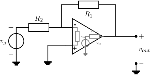
The voltage gain of the configuration of Figure 7.3 can be easily obtained if we assume and :
For the signal transfer:
The circuit of Figure 7.3 is called an inverting op-amp configuration, since it has a negative voltage gain. Other characteristics of the circuit are covered below; again it is assumed for simplicity that and .
The input resistance of this circuit can be calculated in various ways; one of those methods is driving the input by and deriving the input current , after which :
This last expression for is correct, but also quite ugly. There are (infinitely) many ways of writing this equation, where some representations are more “readable” than others. A few examples are given below:
The latter form is very readable, and shows that for a large , the input resistance almost equals . If we let , then the equation simplifies to:
First obtaining the complete answer and subsequently substituting gives the correct answer, but it is much easier to assume a priori. In that case (for a finite output voltage), the differential input voltage will be V. This simplifies the derivation to:
A different but simple derivation can be performed by acknowledging that the input resistance of the circuit is equal to the sum of , and the input resistance as seen on the -input of the op-amp.
The output resistance of the inverting op-amp circuit can be calculated in many ways, all working towards Ohm’s Law applied to the output port of the system. Driving the output port with an independent signal source yields:
It would be great if you’ve just experienced a déjà vu, since this derivation is almost identical to that of the non-inverting amplifier, a few pages back. Here, we again “see” the resistance of the circuit at the output, parallel to the output resistance of the op-amp, decreased by a factor . The output resistance is very low for a high or for a low .
The inverting amplifier was covered in §7.2.2. For this circuit, the +-input of the amplifier was grounded, and the potential of the -input was almost equal to 0 V. Because the potential at the -input is almost at ground potential, though it is not actually grounded, this (type of) node is usually referred to a virtual ground. We analyse a number of issues for the part of the inverting amplifier on the right hand side of , see Figure 7.4.
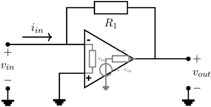
The input impedance of the circuit in Figure 7.4 is (with ):
So, for a large , this input resistance is very low. For the limit case that , the input impedance is . The interesting part of this virtual ground node is that the (total) input current “sees” a low impedance, while this current is forced through an arbitrary impedance (here ). This means that the circuit can function as a current-to-voltage converter: the input current sees an ideal (low impedance) input resistance and the input current is converted to an output voltage via .
The phenomenon from the previous section can also be described using the Miller-effect[8]. Generalizing the resistance in the circuit of Figure 7.4 to an impedance , the voltage drop across this equals . The input impedance due to the combination of the amplifier with voltage gain and the feedback impedance is:
Using a feedback resistor across a voltage amplifier with gain results in a low input resistance for the circuit in Figure 7.4. Similarly, using a feedback capacitor results in a low input impedance, which corresponds to a high input capacitance . Note that when wrapping this kind of feedback around a non-inverting amplifier it is also possible to create negative input resistances, negative input capacitances and more useful stuff.
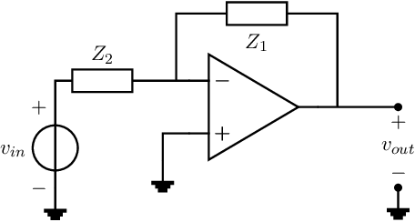
There is a variety of interesting frequency-dependent linear applications for the op-amp. One of the most simple applications is the integrator. For the configuration of Figure 7.5, we assume the op-amp to be ideal, meaning that and and . For this circuit, the output signal is
in the frequency domain and in time domain respectively.
The relation of an integrator in time domain is something like . By equating this to (7.4), it follows that an integrator can be created by:
These two generalizations are presented in Figure 7.6; a derivation of the relation between the input and output voltage is given below for the integrator using a capacitor. Obviously, the derivation for the integrator circuit with an inductor is very similar.
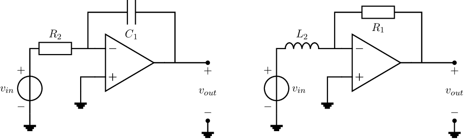
Substitution of the impedances in (7.3) yields an expression for an integrator in frequency domain: . From this it can be concluded that the term corresponds to integration.
After the explanation, derivation, realization and obtaining some general knowledge of interesting facts considering the integrator, it may come to no surprise that we can also create differentiators with an op-amp circuit. Just like in §7.2.5, we can create a relation with the circuit in Figure 7.5 by:
The two situations are given in Figure 7.7. A derivation of the large-signal transfer is given below. The derivation for the differentiator with an inductor is completely analogous.
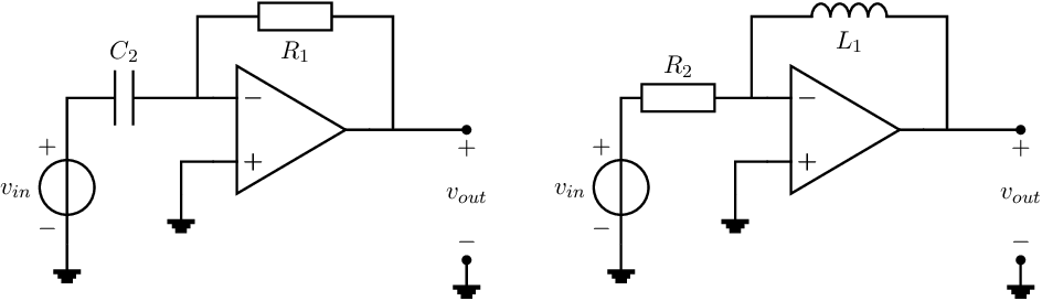
Again, substitution of the (frequency domain) impedances in (7.3) yields an expression for a differentiator in frequency domain: . From this it can be concluded that the term corresponds to differentiation; in Laplace transformation it is written as . Note that both the circuit configurations and the transfer functions are their exact complement.
Summing currents is fairly easy, according to Kirchhoff’s current law: the summed current flowing out of a node is equal to the sum of the currents flowing into that node. The only thing we need is a node that can drain the summed current: a zero-impedance node, and an output that gives some useful information about this summed current.
In §7.2.3, an op-amp circuit that converts an input current to an output voltage was discussed. For this circuit, the input node is virtual ground (very low ohmic). The circuit in Figure 7.4 can be reused to create a circuit that sums currents by only applying multiple input current sources, see the figure below:
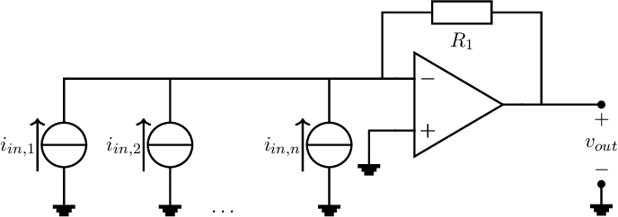
It can easily be derived that the output voltage can be written as . Subtracting currents is just as easy by reversing the direction of an input current source. Changing current directions can, for instance, be done with a current mirror if we are using a unipolar current.
Adding voltages is quite easy if all the voltages are “floating”, i.e. if the terminals of the sources that provide the voltages to add are not referred to any other voltage level. In reality, this is however hardly ever the case. Noting that summing current is easy using the circuit in Figure 7.8, summing voltages can be done by first doing a V-I conversion and then using the current adder circuit in §7.2.7:
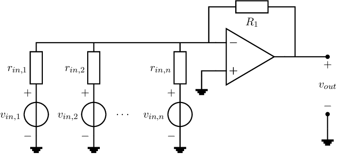
The circuit in Figure 7.9 consists of linear voltage-to-current converters (resistors), a current summation point (virtual ground point created by an op-amp with feedback) and a current-to-voltage converter (resistor ). The transfer function can easily be determined (again with an ideal op-amp), for example using superposition:
If all input conversion resistors are equal, then the relation above simplifies to
The transfer can also be calculated using a non-ideal op-amp, but then the calculations become somewhat more complex.
As briefly discussed in §7.2.7, changing a current adder into a current subtractor is fairly straightforward. Subtracting voltages can be realized in a number of ways:
The latter method is generally used and results in the circuit in Figure 7.10.
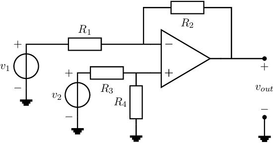
The signal transfer of this circuit can easily be determined by using the principle of superposition. By assuming (for simplicity) :
To ensure to be proportional to , the next equation must be satisfied:
| (7.5) |
resulting in a signal transfer given by
| (7.6) |
The input resistance of both inputs can again be calculated fairly easily by assuming . The input resistance “seen” by source equals ; the input resistance “seen” from source is equal to . We can make these input resistances equal by choosing a proper value for and . Simple math then results in:
| (7.7) |
| (7.8) |
The output impedance of the circuit in Figure 7.10 is quite relevant if the circuit drives something else, which is always the case. For an op-amp with feedback and , it is straight forward to derive that the output resistance is always
Analog filters are required for many different applications46 . First-order filters can be constructed very easily using op-amps: a cascade of a first-order RC filter or a first-order RL filter and a unity gain voltage buffer stage using an op-amp does the job. The op-amp then takes care of a high ohmic load for the filter, while its low output impedance enables driving other circuitry without changing the filter characteristics47 .
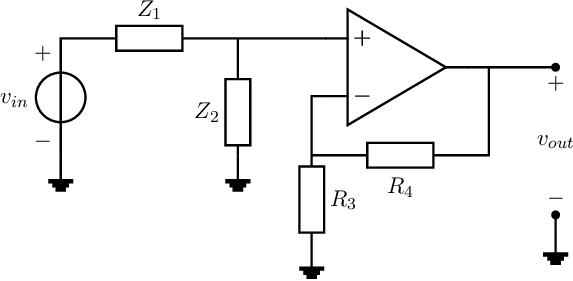
Using an ideal op-amp, the transfer function of the circuit in Figure 7.11 is:
Using this principle, we can create a number of different filters. Usually, such filters have only one reactive element (C or L), resulting in a first-order filter. In general, the possibilities are:
Higher order filters can be easily constructed using cascades of first order and second order filters. The work by Sallen and Key [9] is well known for creating op-amp based filters.
Figure 7.11 shows the topology of a simple first order filter, wrapped around an opamp. For a generic -order filter, it can be shown that its transfer can be rewritten in a cascade of and -order sections. This latter may not be simplified to a cascade of first-order transfers due to requiring real values corner frequencies.
To simplify the design of second order filters wrapped around an opamp (here), many easy-to-use standard configurations are available in literature. The most widely known are the so-called Sallen and Key [9] configurations. The basic topologies for the second order low-pass and high-pass filter configurations are shown below.
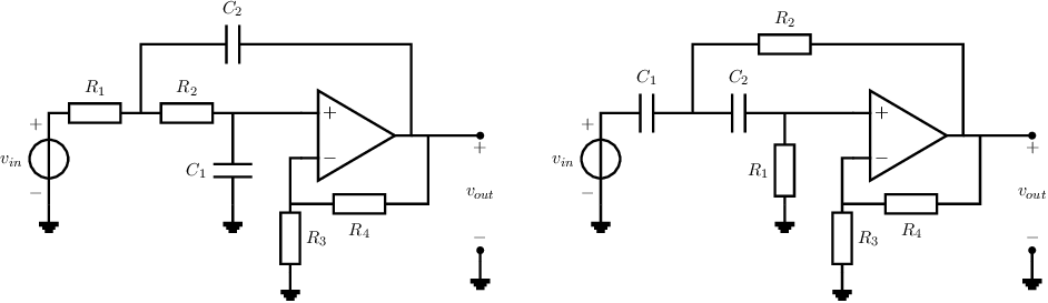
Sallen and Key derived the transfer function, and rewrite that in a corner-frequency-independent form. Also rules to transform a low-pass filter into e.g. a high pass filter are provided by Sallen and Key. Below, a short review of only the low pass filters is provided. For the 2-order low pass configuration:
This set of equation can be used in multiple ways to get a filter with (radian) corner frequency and quality factor . Using and simplifies the design procedure quite a bit as then
The only thing left is now to determine the and for the first and second order parts that make up your order filter. These and depend on the type of filtering characteristic you aim for. Well known characteristics include the Butterworth, Bessel and Chebyshev characteristics that yield a maximally flat frequency response in the passband, a smooth phase transition and a maximum steepness respectively. The and can be calculated from the characteristic polynomials for specific filter characteristics; below the polynomials for low-pass Butterworth filters are shown in Laplace notation with the frequency normalized to 1 rad/s.
| order | polynomial |
| 1 | |
| 2 | |
| 3 | |
| 4 | |
| 5 | |
| 6 | |
The mapping of these polynomials on normalized
and can
easily be derived:
| order | FSF | Q | FSF | Q | FSF | Q |
| 1 | 1.0 | |||||
| 2 | 1.0 | 0.7071 | ||||
| 3 | 1.0 | 1.0000 | 1.0 | |||
| 4 | 1.0 | 0.5412 | 1.0 | 1.3065 | ||
| 5 | 1.0 | 0.6180 | 1.0 | 1.6181 | 1.0 | |
| 6 | 1.0 | 0.5177 | 1.0 | 0.7071 | 1.0 | 1.9320 |
This table should be read as follows:
Whereas for Butterworth filters the corner frequency of each individual section equals that of the overall filter, this is not the case for other filter characteristics. As example, the table below shows the for a Chebyshev filter with a maximum 1dB ripple in the pass band. Note here that FSF may deviate quite a bit from 1:
| order | FSF | Q | FSF | Q | FSF | Q |
| 1 | 0.5088 | |||||
| 2 | 1.0500 | 0.9565 | ||||
| 3 | 0.9971 | 2.0176 | 0.4942 | |||
| 4 | 0.9932 | 0.7845 | 0.5286 | 3.5600 | ||
| 5 | 0.9941 | 1.3988 | 0.6652 | 5.5538 | 0.2895 | |
| 6 | 0.9953 | 0.7608 | 0.7468 | 2.1977 | 0.3532 | 8.0012 |
Transforming the characteristic polynomials into high pass filters is relatively easy: replacing by , which is based on the symmetry (in a Bode plot, with respect to the frequency axis) between the low pass and high pass transfer functions. A lot more to write and say about filter design, but way too little space and time.