Exercise 11.4 An RF amplifier
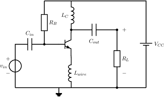
The circuit schematic in the figure below is a more of less regular common emitter amplifier. The circuit contains two
inductors; is an
explicit inductor while
is the inductor that models the wire between emitter and ground. This is the only wired modelled in this
question.

-
a)
- Assuming that ,
derive the voltage gain of this circuit, including load
.
For now,
- the capacitors can be assumed to be low ohmic at signal frequencies
- the impedance of
can be assumed to be much larger than
-
b)
- Including ,
derive the voltage gain of this circuit, including load
.
For now,
- the capacitors can be assumed to be low ohmic at signal frequencies
- the impedance of
can be assumed to be much larger than
-
c)
- Now for ,
and ,
,
derive the (bias)
and the
of the transistor.
-
d)
- Using the values in the previous question, calculate the numerical value of the decrease in
voltage gain due to 1 cm wire (making up
at 100 MHz. You may use the rule-of-thumb wire inductance of 1nH/mm.
-
e)
- As explained before, any junction can be associated with a (voltage dependent) capacitance.
Taking into account only the capacitance associated with the base-emitter junction, ,
and assuming for now ,
derive an expression for voltage gain.

