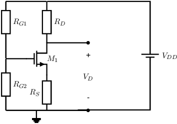
Exercise 3.7 Biasing a circuit with an NMOS transistor
In the circuit schematic below, transistor
is to be biased at a drain current .

-
a)
- Derive an expression for the value of ,
required to set a drain current ,
as a function of properties of the components in the circuit (resistor values, transistor parameters,
supply voltage, ...).
-
b)
- Calculate the numerical value of
for ,
,
,
,
,
.
Note: you can also answer this question if you didn’t answer a) (yet). In that case, explain each
step in your calculation.
-
c)
- We use the circuit with the values above as an amplifier, where
will be the output voltage. Therefore we want to maximize the voltage swing at the
node. Derive and equation AND derive the numerical value of
for maximum voltage swing such that the output signal will not clip to the supply or push
out of saturation.

