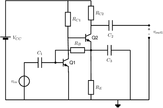
Exercise 5.8 An amplifier with 2 NPNs
The next figure shows the circuit schematic of an amplifier consisting of two stages. For the
signal frequencies of interest all capacitors may be considered as low ohmic. For both transistors
.
You can assume that the base-emitter voltages of the transistors are equal to
.

The circuit is dimensioned for operation at a
power supply (). Both transistors
are biased at a collector current of .
-
a)
- As extra information: the bias voltage at the emitter of
is chosen to be .
Calculate the required values for ,
and .
-
b)
- Draw the small signal equivalent circuit of the
amplifier stage, and use it to calculate the input resistance of this stage (seen at the base of
).
-
c)
- Derive an expression for the voltage gain of the complete two-stage amplifier, that is from
to .
Do not yet insert values, that is give your answer as a function of e.g. ,
,
,
,
,
,
etc.
-
d)
- Calculate the value of
required for a total voltage gain of .
Assume that all other component values are known.

