Exercise 5.2 A weird degenerated amplifier with an NPN
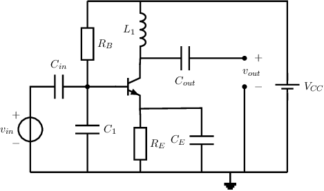
Given is the circuit schematic below. The transistor in this schematic has current gain
and
has a finite output resistance; the collector current can be written as:
|
|
with the Early Voltage,
(Boltzmann constant)
and (elementary charge).
Consequently, at room
temperature, . You can
assume the components ,
, and
to be
“large” for the signal frequencies of interest. We will ignore the output impedance of the BJT for all sub
questions except for (d).

-
a)
- Derive an expression for the bias collector current
expressed in properties or values of the various components. Do not neglect the base current.
-
b)
- Find an expression for the bias collector voltage .
-
c)
- What amplifier topology is this (no motivation needed)?
-
d)
- Explain what you have to assume to be able to neglect the output impedance of the BJT in
small signal derivations of e.g. voltage gain and output impedance.
-
e)
- Draw a small-signal equivalent circuit of this amplifier.
-
f)
- Calculate the output impedance of this amplifier.
-
g)
- Calculate the small-signal voltage gain of this amplifier.

