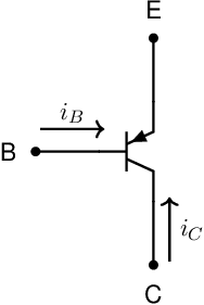
The figure below shows the symbol of a PNP transistor, identifying its emitter (E), base (B) and collector (C) nodes. Including all plus and minus signs in the element equations, the I-V relations for this device are:
where is a (negative valued) device property assuming the arrows as shown in the figure and with the listed element equations. Note that a positive conventional current flows opposite of the arrows: out of the base and out of the collector node.
