An answer:
An answer:
A first step can be replacing impedances of pasives with their value at signal frequencies, and setting DC sources to zero.
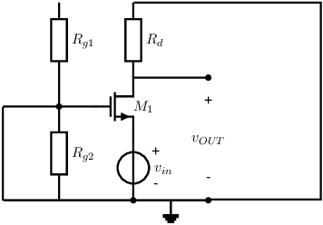
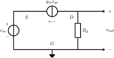
After which a second step can be replacing the non-linear components by their SSEC and cleaning up the schematic. This latter usually is unwinding the (virtual) ground node.
An answer:
An answer:
Applying Ohm’s law to the input port and (re)using the input voltage source to drive input port:
An answer:
Assuming a current source driving the output port: